Structure and preparation method of surface electric field enhanced PIN photoelectric detector

A photodetector, surface electric field technology, applied in circuits, electrical components, semiconductor devices, etc., can solve the problems of reducing the spectral response of the detection device, reducing the spectral response of the short-wave band, and reducing the efficiency of carrier collection, and improving the spectral response. , Improve the collection efficiency and increase the effect of the back electric field strength

Active Publication Date: 2013-11-20
BEIJING UNIV OF TECH
View PDF7 Cites 17 Cited by
  • Summary
  • Abstract
  • Description
  • Claims
  • Application Information

AI Technical Summary

Problems solved by technology

The entire surface of the former adopts a p-type heavily doped region, which improves the collection efficiency of the detector by increasing the electric field strength of the depletion region, but the doping concentration of the p-type heavily doped region is usually within 10 19 cm -3 Above, the thickness reaches more than 1 micron, which will introduce damage, generate a large number of non-radiative recombination centers, greatly reduce the minority carrier lifetime (about 1 microsecond), and greatly reduce the spectral response of the short-wave band
The entire surface of the latter uses a thinner p-type lightly doped region, and the doping concentration is usually 10 16 cm -3 Around, the thickness is below 0.5 microns, although the minority carrier lifetime (about 100 microseconds) is improved and the response in the short-wave band is improved, but after the photo-generated holes are collected into the p-type lightly doped region, they still have to go through a long lateral The transport process can only be collected by the electrode, and the response speed is slow. At the same time, the non-radiative recombination caused by the interface states on the surface further reduces the spectral response of the detection device.
[0004] figure 1 (a) shows the physical process of photogenerated carrier collection in traditional structure photodetectors, since the traditional structure photodetector only has p-type lightly doped region 105, except through process ①, near the p-type ohmic contact layer 104 The photogenerated holes can be directly collected by the p-type ohmic contact electrode 102, and the rest of the photogenerated holes collected by the p-type lightly doped region 105 need to be transported laterally for a long distance to reach the p-type ohmic contact layer 104, and then be collected by the p-type ohmic contact layer 104. The ohmic contact electrode 102 collects, as shown in the process ② in the figure, because there are many interface states at the interface, the photogenerated holes are very prone to non-radiative recombination in the process ②, resulting in a decrease in carrier collection efficiency and a decrease in the spectral response of the device

Method used


Image

  • Structure and preparation method of surface electric field enhanced PIN photoelectric detector
  • Structure and preparation method of surface electric field enhanced PIN photoelectric detector
  • Structure and preparation method of surface electric field enhanced PIN photoelectric detector

Examples


Embodiment Construction

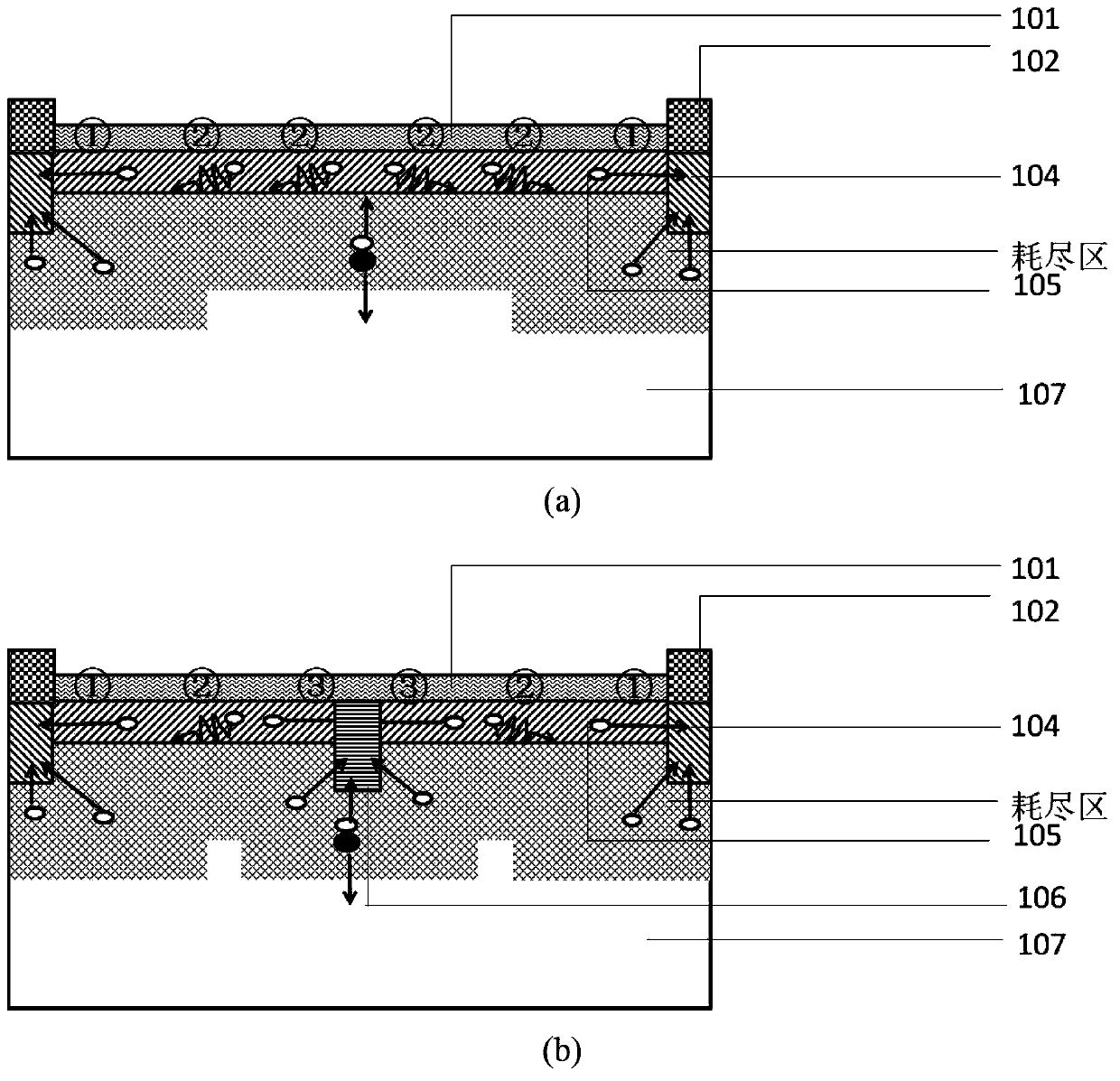
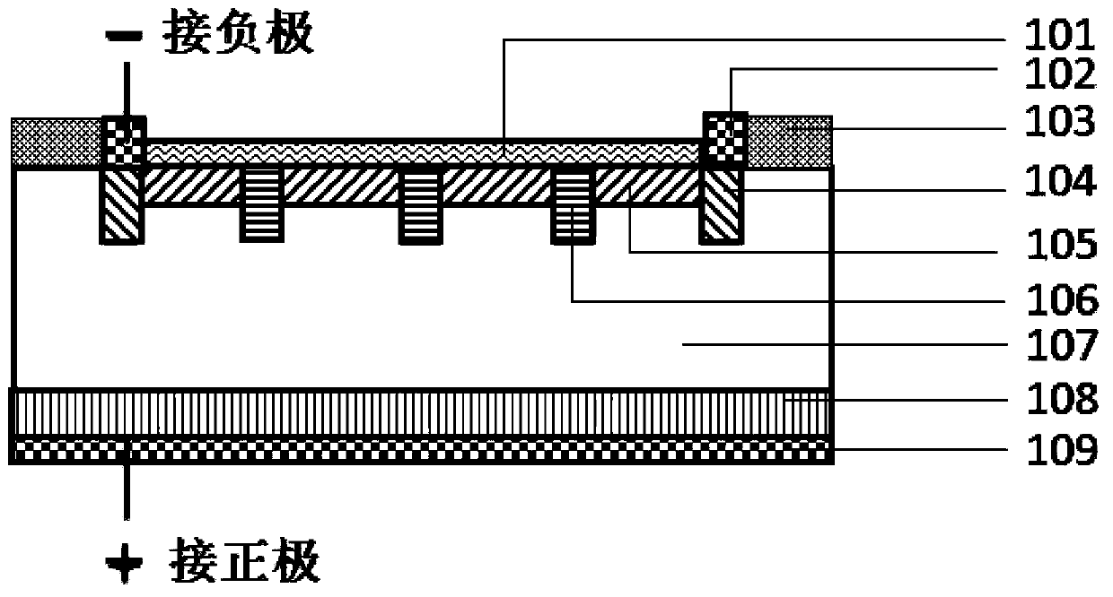
[0031] as attached Figure 5 As shown, the intrinsic layer 107 is made of n-type doped high-resistance silicon material with a doping concentration of 5×10 11 cm -3 , and taking the p-type heavily doped lattice as an example, the preparation process and method are as follows:

[0032] 1. Thermal oxidation or growth of an oxidation protection layer 103 on the surface of the n-type high resistance silicon intrinsic layer 107;

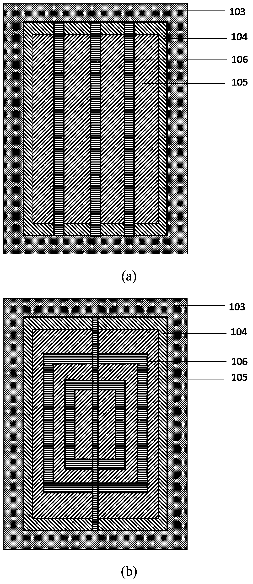
[0033] 2. Photoetching out the pattern of p-type ohmic contact layer 104 and p-type heavily doped lattice 106, etching the front oxidation protection layer 103, injecting boron on the front side of n-type high-resistance silicon intrinsic layer 107 to form p-type ohmic contact Layer 104 and p-type heavily doped lattice 106, the doping concentration is 5×10 19 cm -3 , the depth is 2 μm, the top view of the p-type heavily doped lattice 106 is a square lattice, the length and width are both 20 μm, and the strip width connecting the p-type heavily doped l...


PUM


Abstract

The invention relates to a structure and a preparation method of a surface electric field enhanced PIN photoelectric detector, and belongs to photoelectric detectors. The PIN photoelectric detector is characterized in that a p-type heavily doped region 106 is selectively added in a single p-type lightly doped region 105 which originally covers the whole photosensitive surface, the p-type heavily doped region 106 is enabled to be connected with a p-type ohmic contact layer, thereby enabling a longitudinal electric field to be enhanced, improving the response speed of the detector, introducing a transverse electric field at the same time, increasing transport channels of photoproduction holes, reducing the transport resistance, reducing nonradiative recombination when the photoproduction holes are transported to an electrode in the p-type lightly doped region 105, improving the collection efficiency of the photoproduction holes, and then effectively improving the quantum efficiency. The structural design and the preparation process provided by the invention of the surface electric field enhanced PIN photoelectric detector solve a problem that a photoelectric detector with a traditional structure is low in collection efficiency for photoproduction carriers, and improve the spectral response of devices.

Description

technical field [0001] The invention relates to a structure of a PIN photodetector enhanced by a surface electric field and a preparation method thereof, belonging to the technical field of semiconductor optoelectronics, and relates to a structure of a semiconductor detection device and a preparation method thereof. Background technique [0002] The PIN structure photodetector can effectively increase the absorption length and absorption efficiency. It has the advantages of working at room temperature, high energy resolution, short pulse rise time, high detection efficiency, and stable performance. It has become a rapid development since the 1960s. It is a kind of semiconductor detector, which is widely used in biomedicine, data storage media, flame monitoring, ultraviolet dose measurement, high-energy ray detection, medical treatment, security inspection, industrial flaw detection and other fields. When light is irradiated on the photosensitive surface of the PIN photodetec...

Claims


Application Information

Patent Timeline
Patent Type & Authority Applications(China)
IPC IPC(8): H01L31/0352H01L31/105H01L31/18
CPCY02P70/50
Inventor 郭霞周弘毅栾信信
Owner BEIJING UNIV OF TECH
Why Eureka
Try Eureka