A kind of preparation method of back-illuminated si-pin photodetector

A photoelectric detector and back-illuminated technology, applied in the field of photoelectric detection, can solve the problems of poor thermomechanical properties, poor crystal quality, and high price, and achieve the effects of low cost, high responsivity, and simple preparation process

Inactive Publication Date: 2016-02-03
UNIV OF ELECTRONICS SCI & TECH OF CHINA
View PDF3 Cites 0 Cited by
  • Summary
  • Abstract
  • Description
  • Claims
  • Application Information

AI Technical Summary

Problems solved by technology

However, InGaAs single crystal semiconductor materials have disadvantages such as high price, poor thermomechanical properties, poor crystal quality, and not easy to be compatible with existing silicon microelectronics processes.

Method used


Image

  • A kind of preparation method of back-illuminated si-pin photodetector
  • A kind of preparation method of back-illuminated si-pin photodetector

Examples


Embodiment Construction

[0040] The present invention will be further described below in conjunction with the accompanying drawings and specific embodiments.

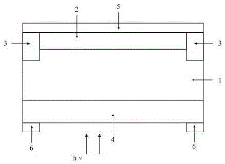
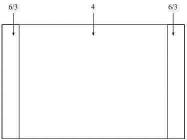
[0041] A back-illuminated Si-PIN photodetector, such as figure 1 , 2 As shown, it includes an I-type substrate 1, a P region 2 disposed above the center of the I-type substrate 1, and a P region located on both sides of the I-type substrate 1 and adjacent to the P region. + Area 3, the N-type nano-microstructure silicon layer 4 located on the back side of the I-type substrate, located in the P-type area 2 and P + The upper end electrode 5 on the upper surface of the region 3 and the lower end electrodes 6 located on both sides under the N-type nano-microstructure silicon layer 4 .

[0042] The N-type nano-microstructure silicon layer is a layered microstructure distributed in a three-dimensional spatial array obtained by performing nanoimprint etching or other nano-etching techniques on heavily diffused phosphorus-doped N regions.

[0043] T...


PUM


Abstract

The invention discloses a back-illuminated Si-PIN photodetector and a preparation method thereof, which relates to a photodetection device structure in the field of photodetection technology, and the photodetector includes an I-type substrate 1, a P region 2, and a P+ region 3. The N region 4 of the nanostructured silicon layer and the upper and lower electrodes, the electrodes include the upper electrode 5 located on the P region 2 and the P+ region 3 and the lower electrode 6 located on the N region 4 of the nanostructured silicon layer. The upper electrode 5 is used for connecting with the cathode of the external circuit; the lower electrode 6 is used for connecting with the anode of the external circuit. This new type of Si photodetector solves the problems of low responsivity and inability to respond to near-infrared bands of traditional Si photodetectors, improves the absorption rate of visible light and near-infrared light, extends the response band to the near-infrared band, and has a higher responsivity. high.

Description

technical field [0001] The invention belongs to the technical field of photoelectric detection, and relates to the structure of a photoelectric detection device, in particular to a back-illuminated Si-PIN photodetector with nano-microstructure silicon as a photosensitive layer and a preparation method thereof. Background technique [0002] As an important part of optical fiber communication system, infrared imaging system, laser warning system and laser ranging system, photoelectric detectors have been widely used in civilian and military applications. Currently widely used photodetectors mainly include Si photodetectors with a detection wavelength range of 400nm~1000nm and InGaAs near-infrared photodetectors with a detection wavelength range of 1000nm~3000nm. Among them, Si material is the most widely used material in the semiconductor industry due to its advantages such as easy purification, easy doping, abundant resources, low cost, easy large-scale integration, and matur...

Claims


Application Information

Patent Timeline
Patent Type & Authority Patents(China)
IPC IPC(8): H01L31/105H01L31/0352H01L31/18
CPCY02P70/50
Inventor 李伟郭安然渠叶君廖家科王冲蒋亚东
Owner UNIV OF ELECTRONICS SCI & TECH OF CHINA
Why Eureka
Try Eureka