Laser cladding printer and manufacturing method of circuit board

A technology of laser cladding and manufacturing methods, which is applied in the direction of laser welding equipment, manufacturing tools, conductive pattern formation, etc., can solve the problems of increasing scrap rate, pollution, increasing cost and pollution, etc., and achieves the effect of simple manufacturing process

Active Publication Date: 2013-12-11
HANS CNC SCI & TECH
View PDF24 Cites 15 Cited by
  • Summary
  • Abstract
  • Description
  • Claims
  • Application Information

AI Technical Summary

Problems solved by technology

Due to the complex process, the whole process requires a lot of manpower, material and financial resources, which makes the production cost of PCB high, and the existence of electroplating, roughening and other processes makes the production process polluting
Coupled with the increasing demand for multi-layer printed circuit boards, the PCB production process needs to be continuously cycled, which increases the scrap rate and increases the cost and pollution

Method used


Image

  • Laser cladding printer and manufacturing method of circuit board
  • Laser cladding printer and manufacturing method of circuit board
  • Laser cladding printer and manufacturing method of circuit board

Examples


Embodiment Construction

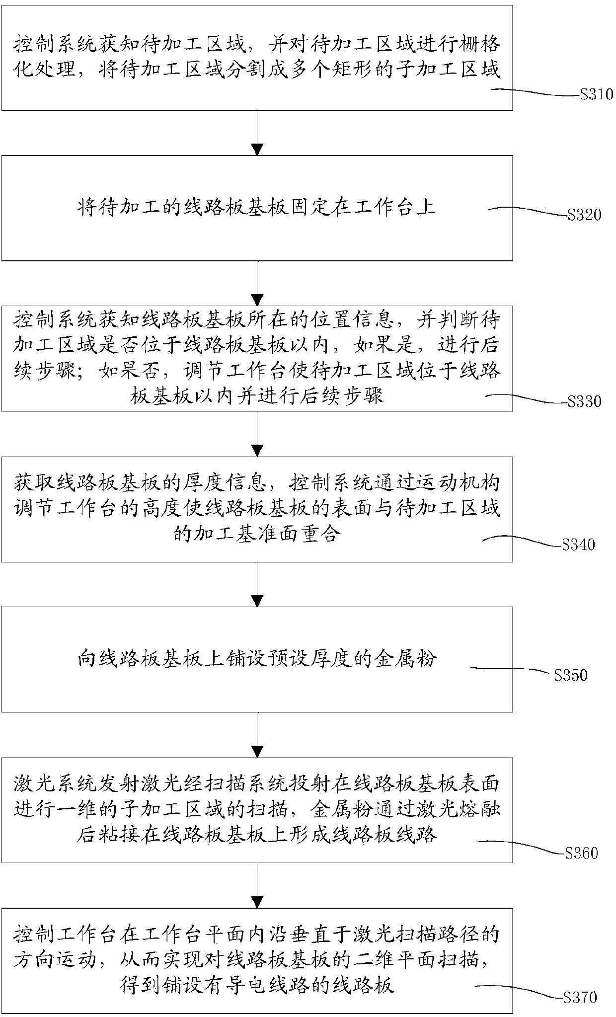
[0025] The laser cladding printer and the manufacturing method of the circuit board using the printer will be further described in detail below in conjunction with the accompanying drawings and specific embodiments.

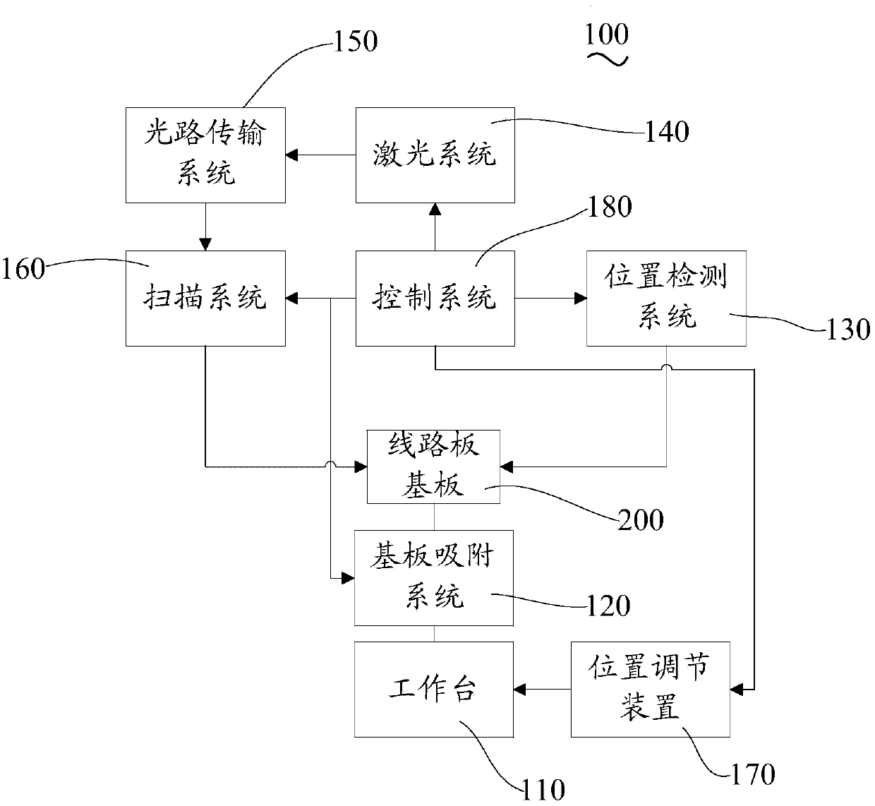
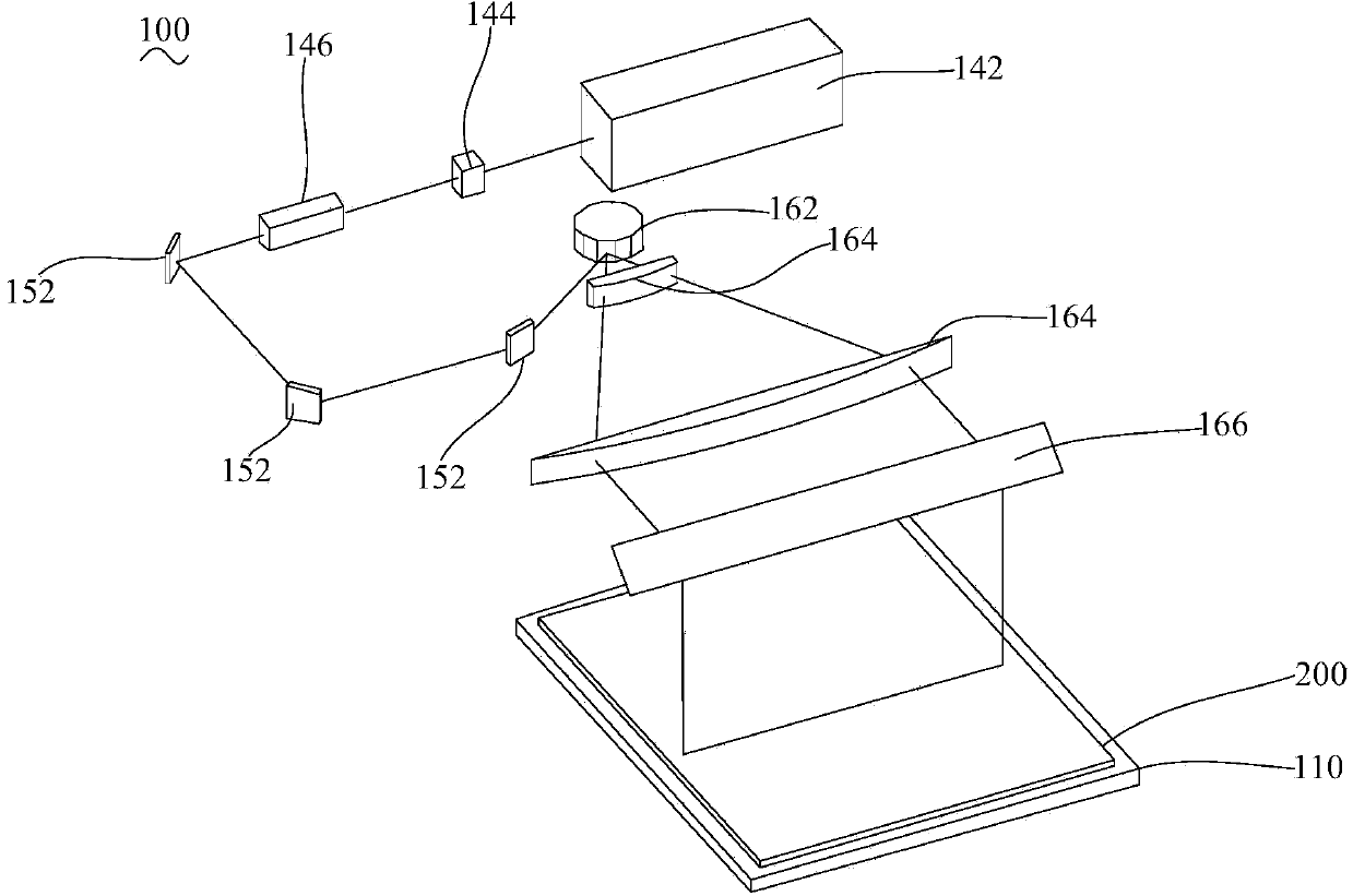
[0026] like figure 1 As shown, the laser cladding printer 100 in one embodiment is mainly used for circuit formation in the circuit board manufacturing process, which includes a workbench 110, a substrate adsorption system 120, a position detection system 130, a laser system 140, an optical transmission system 150, a scanning System 160 , position adjustment device 170 and control system 180 . The control system 180 comprehensively controls the operation of the substrate adsorption system 120 , the position detection system 130 , the laser system 140 , the scanning system 160 and the position adjustment device 170 .

[0027] Please combine the following figure 2 , the workbench 110 is used to carry the circuit board substrate 200 to be processed. The area of ...


PUM

PropertyMeasurementUnit
wavelengthaaaaaaaaaa
thicknessaaaaaaaaaa
pore sizeaaaaaaaaaa

Abstract

The invention relates to a laser cladding printer. The laser cladding printer comprises a worktable, a position detection system, a laser system, a scanning system, a position regulation device and a control system. According to the laser cladding printer, manufacturing procedures of existing partial circuit boards can be replaced, an effect for directly manufacturing circuits of the circuit board through printing the circuit board on high-temperature-resistant substrates such as ceramics, high polymer materials and the like is achieved, the manufacturing process of the circuit board is simple and pollution-free and is low in cost. Besides, the invention further relates to a manufacturing method of the circuit board by utilizing the laser cladding printer.

Description

technical field [0001] The invention relates to the field of circuit board production, in particular to a laser cladding printer made with circuit board circuits and a method for producing a circuit board using the printer. Background technique [0002] With the development of science and technology, the miniaturization and high integration of electronic products have put forward unprecedented high requirements for the production of printed circuit boards (PCB). Although the relevant technologies of PCB board production have been developed rapidly, such as CO 2 The development of laser drilling technology and LDI laser direct imaging technology has injected new impetus into the PCB industry. However, the traditional PCB manufacturing process is complex, including material cutting, pre-processing, image transfer, copper surface roughening, etching, drilling, copper sinking, electroplating, lamination, green painting, molding, etc. Due to the complex process, the whole proce...

Claims


Application Information

Patent Timeline
Patent Type & Authority Applications(China)
IPC IPC(8): B23K26/00B23K26/06B23K26/42H05K3/12
Inventor 陈百强宋福民王星翟学涛杨朝辉高云峰
Owner HANS CNC SCI & TECH
Why Eureka
Try Eureka