Device and process method for preparing polycrystalline silicon through coupling of electron beam smelting and crystal growing technology

A technology of electron beam smelting and process method, which is applied in the direction of chemical instruments and methods, silicon compounds, inorganic chemistry, etc., can solve the problems of increasing overall investment and low production efficiency, and achieve enhanced volatilization effect, improved production efficiency, saving investment and The effect of footprint

Inactive Publication Date: 2013-12-11
QINGDAO XINSHIJI SOLAR ENERGY TECH CO LTD
View PDF4 Cites 9 Cited by
  • Summary
  • Abstract
  • Description
  • Claims
  • Application Information

AI Technical Summary

Problems solved by technology

However, in this process, electron beam smelting technology and crystal growth technology both involve the melting and solidification process of silicon materials. The crystal growth link increases the overall investment, and the production efficiency is low

Method used


Image

  • Device and process method for preparing polycrystalline silicon through coupling of electron beam smelting and crystal growing technology

Examples


Embodiment 1

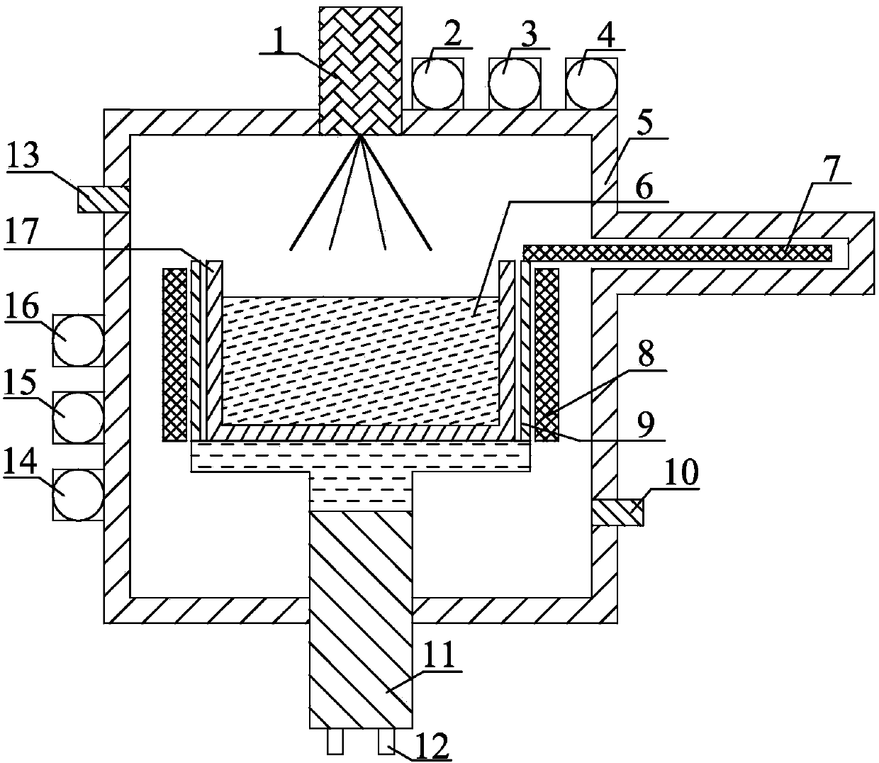
[0029] A graphite crucible 17 is placed inside the furnace body 5, and the inner surface of the graphite crucible 17 is coated with silicon carbide. The outer wall of the graphite crucible 17 is surrounded by a graphite heating body 9 and a graphite insulation cover 8 successively from the inside to the outside. The upper graphite cover plate 7 of the graphite insulation cover 8 can move horizontally, and is parallel to the upper graphite cover plate 7 on one side of the furnace body 5. There is a hollow plate groove outside the position; a water-cooled ingot pulling mechanism 11 is installed at the center of the bottom of the graphite crucible 5; a cooling circulating water pipe 12 is built in it; an electron gun 1 is connected to the top of the furnace body 5, and an inflatable valve 13 is opened on the upper end of the side. The lower end is provided with an air release valve 10.

Embodiment 2

[0031] Using the device in Example 1 to couple electron beam smelting and crystal growth technology to prepare polysilicon:

[0032] (1) Clean 500kg of polysilicon materials with a phosphorus content of 0.005%, a metal content of 0.00009%, and a boron content of 0.000014% with cleaning equipment to remove dust and oil stains on the surface, put them in a drying box, and dry them at 80°C Put the dried silicon material into the graphite crucible 17, move the graphite crucible 17 into the equipment for positioning; put the graphite crucible 17 into the graphite heating body 9, and the graphite heating body 9 is added with a graphite insulation sheath 8 to play Insulation effect.

[0033] (2) Put the equipment together, turn on the equipment cooling and circulating water device, and pass the cooling and circulating water to the equipment through the cooling and circulating water pipe 12; open the vacuum system of the furnace body, first use the mechanical pump 14 and the Roots pum...

Embodiment 3

[0040] Using the device in Example 1 to couple electron beam smelting and crystal growth technology to prepare polysilicon:

[0041] (1) Clean 500kg of polysilicon materials with a phosphorus content of 0.005%, a metal content of 0.00008%, and a boron content of 0.000013% with cleaning equipment to remove dust and oil stains on the surface, put them in a drying box, and dry them at 80°C dry; the dried silicon material is put into the graphite crucible 17, and the graphite crucible 17 is moved into the equipment for positioning; the graphite crucible 17 is put into the graphite heating body 9, and the graphite heating body 9 is added with a graphite insulation sheath 8, and the to the heat preservation effect.

[0042] (2) Put the equipment together, turn on the equipment cooling and circulating water device, and pass the cooling and circulating water to the equipment through the cooling and circulating water pipe 12; open the vacuum system of the furnace body, first use the me...


PUM


Abstract

The invention belongs to the field of polycrystalline silicon ingot, and particularly relates to a device and a process method for preparing polycrystalline silicon through the coupling of electronic beam smelting and the crystal growing technology. The device for preparing the polycrystalline silicon through the coupling of the electron beam smelting and the crystal growing technology is characterized in that a graphite crucible is arranged inside a furnace body, the outer wall of the graphite crucible is sequentially provided with a graphite heating body and a graphite insulating sleeve from inside to outside, an upper graphite cover plate of the graphite insulating sleeve can be horizontally moved, and the position on one side of the furnace body, parallel to the upper graphite cover plate, is externally connected with a hollow plate groove; a water-cooling ingot pulling mechanism is installed on the center position of the bottom of the graphite crucible; a cooling circulating water pipe is arranged inside the water-cooling ingot pulling mechanism; the top of the furnace body is provided with an electron gun, the upper end of the side part of the furnace body is provided with an inflating valve, and the lower end is provided with a deflation valve. The process method for preparing the polycrystalline silicon through the coupling of the electron beam smelting and the crystal growing technology comprises the steps of filling materials, vacuumizing, charging argon to increase the pressure, heating to smelt the silicon material, smelting through an electron beam, growing the crystal, annealing the ingot, cooling and opening the furnace to take the ingot.

Description

technical field [0001] The invention belongs to the field of polycrystalline silicon ingots, and in particular relates to a device and a process method for preparing polycrystalline silicon by coupling electron beam smelting and crystal growth technology. Background technique [0002] Metallurgical preparation of solar-grade polysilicon technology, as the only way to develop low-cost and environmentally friendly solar-grade polysilicon preparation technology, has achieved considerable development and achieved industrial production. Purification of polysilicon by metallurgical method refers to the method of removing various impurity elements (phosphorus, boron and metal) in silicon in sequence without silicon participating in chemical reactions by means of physical metallurgy. It is not a single preparation method, but An integrated method, which mainly uses the principle of saturated vapor pressure, segregation and oxidative difference, and uses different processes to remove...

Claims


Application Information

Patent Timeline
Patent Type & Authority Applications(China)
IPC IPC(8): C01B33/037
Inventor 谭毅郭校亮安广野姜大川
Owner QINGDAO XINSHIJI SOLAR ENERGY TECH CO LTD
Why Eureka
Try Eureka