A surface treatment method that can control the carrier concentration of carbon-based semiconductor devices

A carrier concentration and surface treatment technology, applied in the field of nanoelectronics, can solve the problems of large structural damage of carbon materials and decreased carrier mobility of materials

Active Publication Date: 2016-06-29
INST OF MICROELECTRONICS CHINESE ACAD OF SCI
View PDF7 Cites 0 Cited by
  • Summary
  • Abstract
  • Description
  • Claims
  • Application Information

AI Technical Summary

Problems solved by technology

[0005] In view of this, the main purpose of the present invention is to provide a surface treatment method that can regulate the carrier concentration of carbon-based semiconductor devices, so as to solve the problem that conventional displacement doping and implantation doping can greatly damage the structure of carbon materials, resulting in The problem of a significant drop in material carrier mobility

Method used


Image

  • A surface treatment method that can control the carrier concentration of carbon-based semiconductor devices
  • A surface treatment method that can control the carrier concentration of carbon-based semiconductor devices
  • A surface treatment method that can control the carrier concentration of carbon-based semiconductor devices

Examples


Embodiment 1

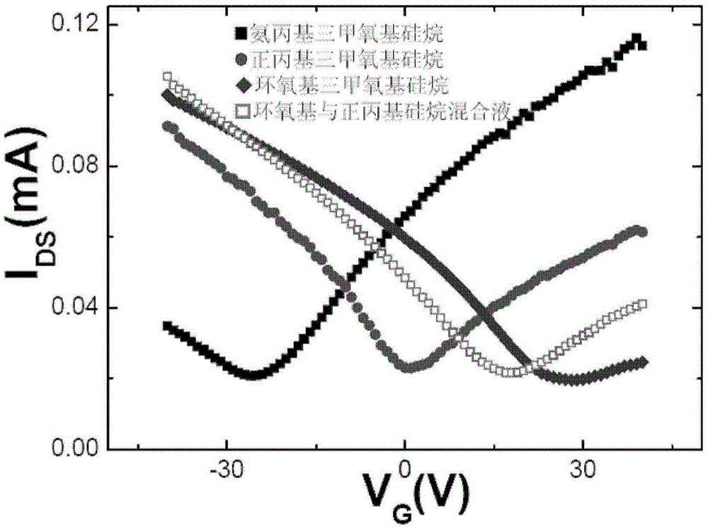
[0034] Embodiment 1: use CVD to grow graphene material, on the silicon dioxide / silicon substrate after n-propyltrimethoxysilane is processed film formation, realize graphene field effect transistor.

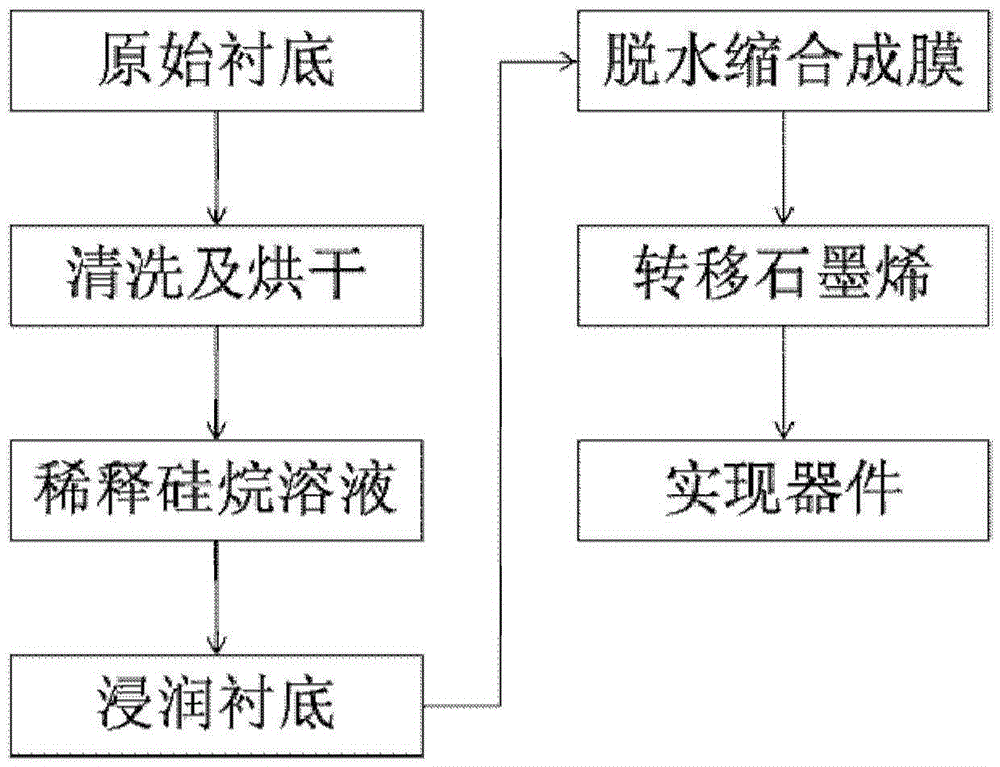
[0035] figure 2 Use silane coupling agent to carry out the flowchart of surface treatment to substrate for the embodiment of the present invention, comprise the following steps:

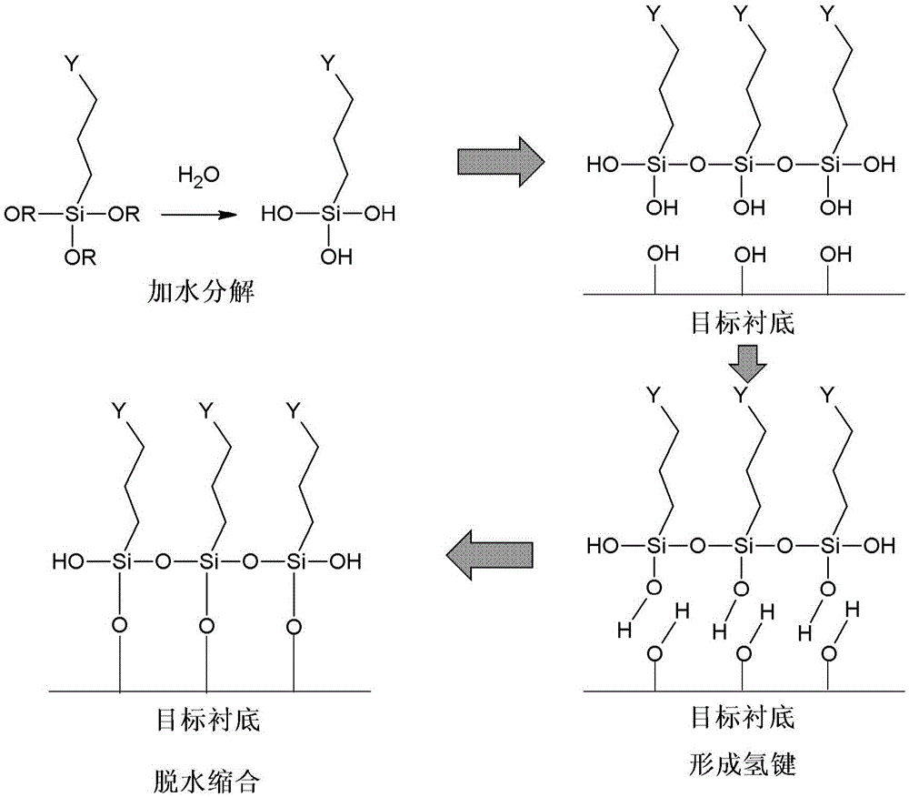
[0036] Step 1: After diluting the silane coupling agent with a solvent, immerse the substrate in the diluted solution. Before immersing, the substrate material needs to be cleaned and baked and dried;

[0037] In this embodiment, the silane coupling agent-n-propyltrimethoxysilane dilution is prepared, and n-propyltrimethoxysilane (purchased from China Pharmaceutical Group Chemical Reagent Beijing Co., Ltd.) and absolute ethanol solution are mixed in volume ratio 1:20-1:400 for dilution, shake well after dilution, immerse the substrate in the silane dilution solution for 1-20 minutes; then put the clea...

Embodiment 2

[0042] Embodiment 2: use CVD to grow graphene material, on the silicon dioxide / silicon substrate after processing film formation through aminopropyltrimethoxysilane, realize graphene field effect transistor.

[0043] The specific steps are similar to Example 1, but in step 1, the dilute solution is prepared with aminopropyltrimethoxysilane and absolute ethanol at a ratio of 1:20-1:400, and the substrate is immersed in the silane diluent for 1-20 minutes . After step 3, measure the thickness of the aminopropyltrimethoxysilane organic film layer to be 1nm-20nm.

Embodiment 3

[0044] Embodiment 3: use CVD growth graphene material, on the silicon dioxide / silicon substrate after (3-oxiranyl methoxy propyl) trimethoxysilane process film formation, realize graphene field effect transistor .

[0045] The specific steps are similar to Example 1, but in step 1, use (3-oxiranylmethoxypropyl) trimethoxysilane and isopropanol to dilute with a volume ratio of 1:20-1:400, and the substrate Wetting deposition time is 1-20 minutes. After step 3, measure the thickness of the (3-oxiranylmethoxypropyl)trimethoxysilane organic film layer to be 1nm-20nm.


PUM


Abstract

The invention discloses a surface treatment method of the carrier concentration of an adjustable controlled carbon-based semiconductor device. The surface treatment method comprises the following steps of forming a silicane organic membrane layer on the surface of a substrate by using a silicane coupling agent, carrying out surface adsorption-type doping on a carbon-based thin-film material attached to the surface of the silicane organic membrane layer by using the different radicals and the nucleophilic and nucleus repellent characteristics in different densities of the silicane organic membrane layer, continuously adjusting the carrier concentration of the carbon-based semiconductor device attached to the surface of the silicane organic membrane layer by adjusting different radical varieties and concentration ratios, and effectively controlling the deviation position of a Dirac point of the carbon-based semiconductor device. The surface treatment method can be used for avoiding the destructive influence on graphene thin-film materials caused by conventional methods such as displacement-type doping and injection-type doping and meanwhile solving the problem of performance degradation of graphene devices caused by polarity scattering, rough fluctuation, impurity adsorption and the like of the surface of the substrate.

Description

technical field [0001] The invention relates to a carbon material-based semiconductor device preparation process, in particular to a surface treatment method capable of regulating the carrier concentration of a carbon-based semiconductor device, and belongs to the technical field of nanoelectronics. Background technique [0002] Nanoelectronics based on carbon materials, especially those based on carbon nanotubes (CarbonNanotube) and graphene (Graphene), are considered to have great application prospects and great potential to replace silicon-based materials. Since the successful development of carbon nanotubes in 1991 and graphene in 2004, carbon-based electronics has made great progress. Carbon-based electronics have attracted more and more attention because of their small size, high speed, low power consumption, and simple process. [0003] For carbon-based semiconductor devices, since the conductive carbon material is only one or a few atomic layers thick, it has an imp...

Claims


Application Information

Patent Timeline
Patent Type & Authority Patents(China)
IPC IPC(8): H01L51/56
Inventor 史敬元金智张大勇麻芃彭松昂
Owner INST OF MICROELECTRONICS CHINESE ACAD OF SCI
Why Eureka
Try Eureka