

Multi-notch ultra wide band antenna
An ultra-wideband antenna and notch technology, which is applied in the field of multi-notch ultra-wideband antennas, can solve the problems of ultra-wideband antenna working frequency band reduction, increase the complexity of antenna design, and cannot filter out interference, so as to reduce design costs and be easy to control , The effect of convenient processing
Inactive Publication Date: 2013-12-11
UNIV OF ELECTRONICS SCI & TECH OF CHINA
View PDF5 Cites 17 Cited by
- Summary
- Abstract
- Description
- Claims
- Application Information
AI Technical Summary
Problems solved by technology
For example, the document "Design of a Band-Notched UWB Monopole Antenna by Means of an EBG Structure, Mohammad Yazdi and Nader Komjani, IEEE ANTENNAS AND WIRELESS PROPAGATION LETTERS, Vol.10, March 2011" uses a mushroom-shaped electromagnetic bandgap structure, A notch in the WLAN frequency band around 5.5GHz is realized, but the antenna uses four EBGs, the antenna is large in size, and cannot filter out the interference of the WiMAX frequency band signal around 3.5GHz
Another example is the document "Narrow Band Notches for Ultra-Wideband Antenna Using Electromagnetic Band-Gap Structures, J.Y.Deng, L.X.Guo and J.H.Yang, Journal of Electromagnetic Waves and Applications, Vol.25, 2011" using two different structures of mushroom-shaped The electromagnetic bandgap structure forms two notch frequency bands of 4.6-5.55GHz and 5.7-6.28GHz, but the bandwidth of the notch frequency band in this document is too wide, far beyond the frequency range of the interference signal, which undoubtedly caused the UWB antenna itself Reduction of working frequency band
Another example is the document "UWB Band-Notched Monopole Antenna Design Using Electromagnetic-Bandgap Structures, Lin Peng and Cheng-Li Ruan, IEEE TRANSACTIONS ON MICROWAVE THEORY AND TECHNIQUES, Vol.59, No.4, April2011", which compared two different structures The electromagnetic bandgap structure realizes notches. Although the bandwidth can be effectively controlled without increasing the volume of the antenna, two structures are required to realize two notches in this structure, which increases the complexity of designing the antenna.
Method used
View moreImage
Smart ImageViewing Examples

Examples
Embodiment
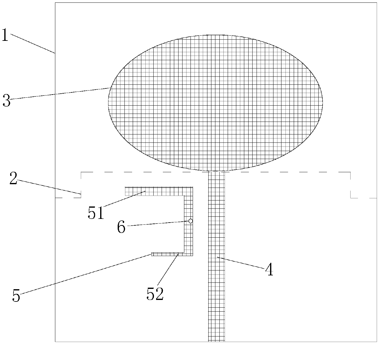
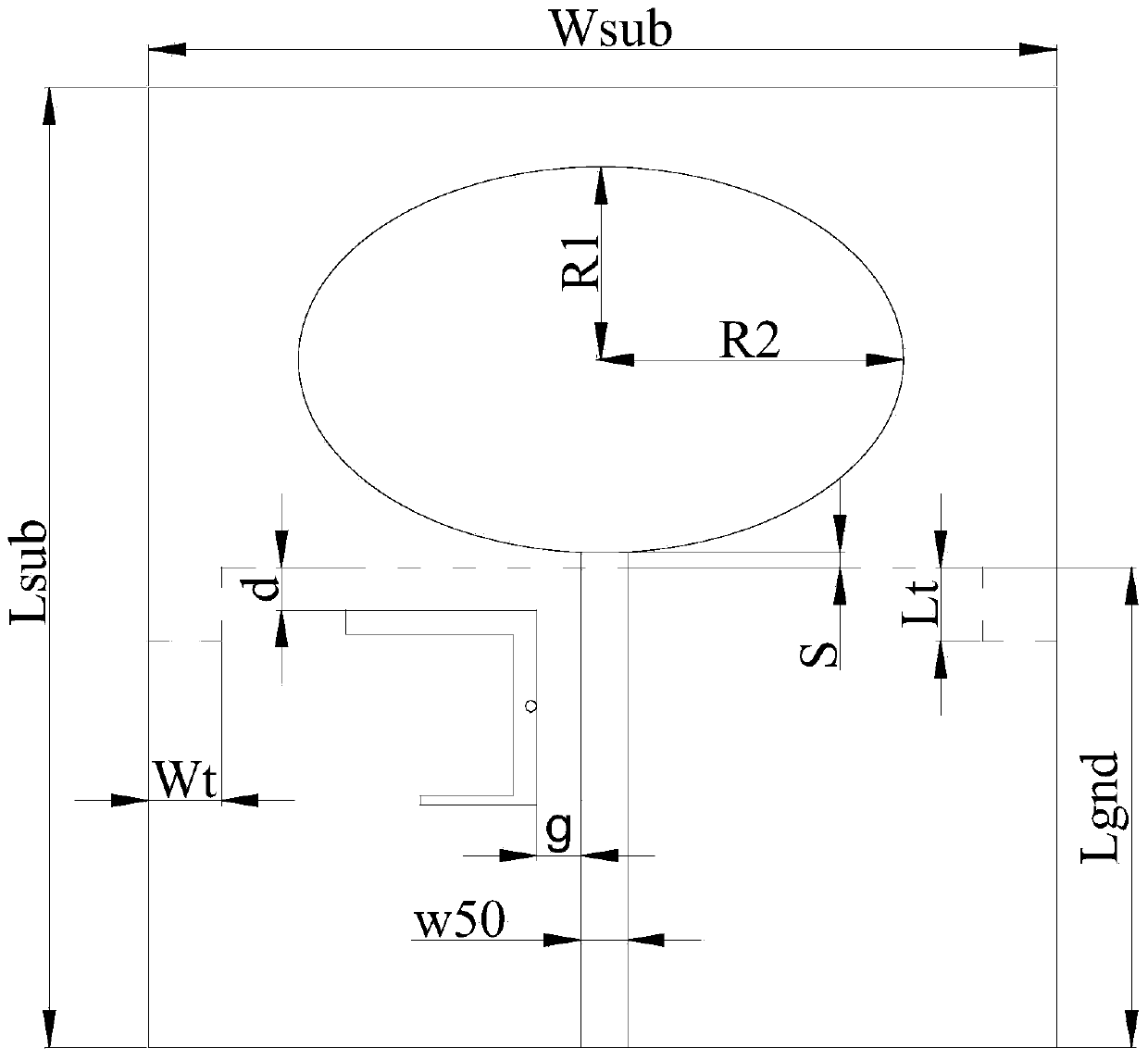
[0035] The specific parameters of the dielectric substrate used in the multi-notch ultra-broadband antenna in this embodiment are relative permittivity εr=4.4 and thickness h=1.0mm. image 3 , Figure 4 It is a schematic diagram of the structural dimensions of the embodiment, and its specific geometric parameters are Wsub=38mm, Lsub=40mm, Lgnd=20mm, R1=8mm, R2=12.8mm, S=0.2mm, d=0mm, w50=1.86mm, Lt =3.0mm, Wt=3.0mm, g=1.0mm, r=0.2mm, W1=1.2mm, L1=8.0mm, W2=0.4mm, L2=4.8mm, W3=1.0mm, L3=8.2mm.
Login to View More PUM
 Abstract
The invention discloses a multi-notch ultra wide band antenna which is simple in structure, small in size, and easy to control and process. The multi-notch ultra wide band antenna comprises a medium substrate, wherein the lower surface of the medium substrate is provided with a metal floor, the upper surface of the medium substrate is provided with a radiation unit and a micro-strip feeder connected with the radiation unit, the upper surface of the medium substrate is provided with an electromagnetic band gap structure formed by a plurality of branches, and the electromagnetic band gap structure is provided with a metal grounding through hole used for grounding. The electromagnetic band gap structure formed by the branches is used to form a notch, the design of a filter is replaced, and design cost and system complexity are reduced, so that the antenna is simple in structure, compact, small, convenient to process, low in cost, easy to produce, good in filtering effect and easy to control. Besides, by means of arrangement of the branches of different numbers, more notch characteristics can be achieved, and the antenna is suitable for being popularized and used in the field of antennas.
Description
technical field [0001] The invention relates to the field of antennas, in particular to a multi-notch ultra-wideband antenna. Background technique [0002] Ultra-wideband technology is a new type of wireless communication technology, which has the characteristics of high transmission rate, low power consumption, low cost, and simple system structure, so it has become one of the research hotspots of wireless communication in recent years. The US Federal Communications Commission (FCC) opened the 3.1GHz-10.6GHz frequency band in 2002 and allowed UWB technology to be used for civilian use. Since then, wireless ultra-wideband technology has received great attention and development. As a key component of wireless communication systems, the design of UWB antennas has become an important factor restricting the capacity and quality of UWB wireless communication channels. Since the frequency band of ultra-wideband is from 3.1 to 10.6GHz, there are inevitably some signal interference...
Claims
Login to View More Application Information
Patent Timeline
 Patent Type & AuthorityApplications(China)
IPC IPC(8): H01Q1/38H01Q1/48
Inventor徐自强刘昊吴波张根夏红廖家轩尉旭波汪澎田忠
OwnerUNIV OF ELECTRONICS SCI & TECH OF CHINA