Double-surface pressing connecting through hole structure of printed-circuit board and machining method thereof

A technology for printed circuit boards and processing methods, which is applied in the directions of printed circuit components, electrical connection formation of printed components, and electrical connection of printed components, which can solve the problems of increased processing difficulty and high thickness, so as to improve wiring density and eliminate parasitic capacitance , beneficial to the effect of integrity

Active Publication Date: 2013-12-18
SHANTOU ULTRASONIC PRINTED BOARD NO 2 FACTORY +1
View PDF6 Cites 21 Cited by
  • Summary
  • Abstract
  • Description
  • Claims
  • Application Information

AI Technical Summary

Problems solved by technology

The circuit board with this structure has a high thickness. After the copper layer thickness required by the customer is completed, the hole diameter will be reduced by more than 70 μm, so that the copper in the small hole can be removed without damaging the copper layer of the crimping holes at both ends, and The hole diameter of the crimping part should be minimized as much as possible, and the processing difficulty will be significantly increased

Method used


Image

  • Double-surface pressing connecting through hole structure of printed-circuit board and machining method thereof
  • Double-surface pressing connecting through hole structure of printed-circuit board and machining method thereof
  • Double-surface pressing connecting through hole structure of printed-circuit board and machining method thereof

Examples


Embodiment

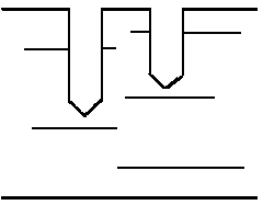
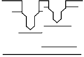
[0057] Example: see Figure 13 , according to the above-mentioned processing method, the double-sided press-through hole structure of the printed circuit board includes a circuit board substrate 1 with a thickness of 6.1mm, and a left hole and a right hole are drilled on the circuit board substrate 1; It is the left crimping hole 3 with a diameter of 0.55mm; the middle part is the left non-metallized small hole 5 with a diameter of 0.35mm; both ends of the right hole are right crimping holes 4 with a diameter of 0.55mm; The metallized small hole 6 has a diameter of 0.35 mm, and the surface of the left crimping hole 3 and the right crimping hole 4 has a 25 μm electroplated copper layer 2; the above-mentioned dimensions can be adjusted according to actual needs.


PUM


Abstract

The invention discloses a double-surface pressing connecting through hole structure of a printed-circuit board and a machining method of the double-surface pressing connecting through hole structure of the printed-circuit board. The machining method comprises the following steps that a small hole A is drilled in the upper surface of a substrate in a depth-control mode; a pressing connecting hole B is drilled in the same position of the small hole A; the substrate is overturned; a small hole C is drilled in the surface opposite to the small hole A in a depth-control mode and is communicated with the small hole A; a pressing connecting hole D is drilled in the position of the small hole C; electroless copper plating, copper electroplating and tinning are carried out; a hole E is drilled in the position of the small hole A in a depth-control mode; the substrate is overturned; a hole F is drilled in the position of the small hole C in a depth-control mode; alkaline etching and tin stripping are carried out; part of a copper layer at each pressing connecting hole is thickened in a plating mode until the design requirement of a finished product is met, and finally the double-surface pressing connecting through hole structure is obtained. The double-surface pressing connecting through hole structure of the printed-circuit board and the machining method of the double-surface pressing connecting through hole structure of the printed-circuit board completely eliminate the stray capacitance among pressing connecting elements, facilitates the integrality of signal transmission and improves wire distribution density; the process is reasonable, the difficulty that plating layers of the middle small holes are eliminated in a drilling mode is largely lowered, and the diameter of the pressing connecting holes is made to be the smallest; the completeness of the plating layers on the walls of the pressing connecting holes is guaranteed, and the non-metallic middle small holes are achieved; copper wire defects in the holes are avoided.

Description

technical field [0001] The invention relates to the field of printed circuit board processing, in particular to a printed circuit board double-sided pressure through-hole structure and a processing method thereof. Background technique [0002] In order to adapt to the development requirements of electronic products towards diversified functions and portability, printed circuit boards have the characteristics of high thickness-to-diameter ratio and high-density fine lines. The lines are getting thinner and the apertures are getting smaller and smaller. Any layer of interconnected circuit boards, the number of layers applied to system circuit boards is gradually increasing and high-speed signal transmission. [0003] Patent application No. 201210379432.9 discloses a "dumbbell" crimping through-hole structure. Both ends of the through-hole of this structure will be crimped. Part, and then use a small diameter drill to process the middle non-crimping part, and use electroless c...

Claims


Application Information

Patent Timeline
Patent Type & Authority Applications(China)
IPC IPC(8): H05K3/42H05K1/11
Inventor 李国有邱彦佳黄函蔡锦松张学东
Owner SHANTOU ULTRASONIC PRINTED BOARD NO 2 FACTORY
Why Eureka
Try Eureka