A three-dimensional interconnect structure and its preparation method
A three-dimensional interconnection and metal wiring layer technology, which is applied in semiconductor/solid-state device manufacturing, semiconductor/solid-state device components, semiconductor devices, etc., can solve the problems of high-speed and high-frequency transmission performance, and achieve small signal reflection and medium Less loss, good high-frequency performance
- Summary
- Abstract
- Description
- Claims
- Application Information
AI Technical Summary
Problems solved by technology
Method used
Image

Examples
Embodiment 1
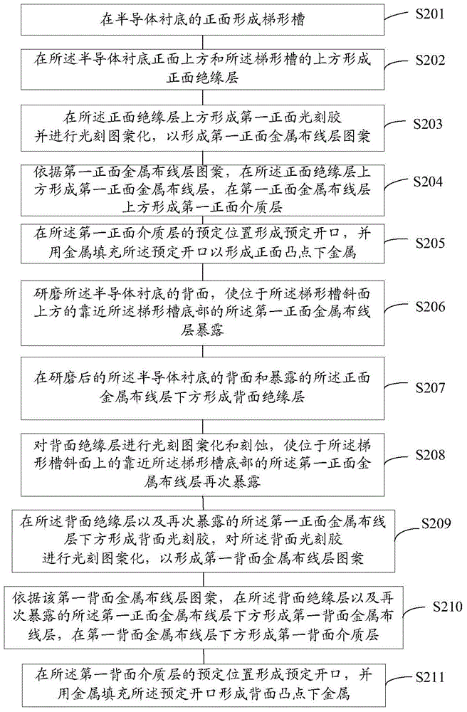
[0069] combine Figure 2 to Figure 3 (11) The manufacturing method of the first embodiment is described in detail. The preparation method of the three-dimensional interconnection structure described in the first embodiment includes the preparation of a front metal wiring layer and a back metal wiring layer. figure 2 is a schematic flow chart of the manufacturing method of this embodiment, Figure 3(1) to Figure 3(11) It is a structural diagram corresponding to a series of manufacturing processes of the manufacturing method of this embodiment.
[0070] see figure 2 , the production method includes the following steps:
[0071] S201, forming trapezoidal grooves on the front surface of the semiconductor substrate;
[0072] In the semiconductor manufacturing process, the etching region formed by selective etching or anisotropic etching is generally a groove with a wide top and a narrow bottom, generally a trapezoidal groove. The selective etching is generally dry etching, s...
Embodiment 2
[0108] The method for preparing the three-dimensional interconnection structure described in the second embodiment includes preparing two layers of front metal wiring layers and two layers of back metal wiring layers. It can be understood that those skilled in the art can also obtain three or more front metal wiring layers and back metal wiring layers according to the method of preparing two front metal wiring layers and two back metal wiring layers. Embodiment 1 has many similarities with Embodiment 2. For the sake of brevity, this embodiment only focuses on the differences. For the similarities, please refer to the description of Embodiment 1.
[0109] combine Figure 4 to Figure 5 (14) The preparation method of this example is described. The preparation method of the three-dimensional interconnection structure comprises the following steps:
[0110] Steps S401 to S403 are the same as steps S201 to S203 in the first embodiment, and for the sake of brevity, no detailed desc...
Embodiment 3
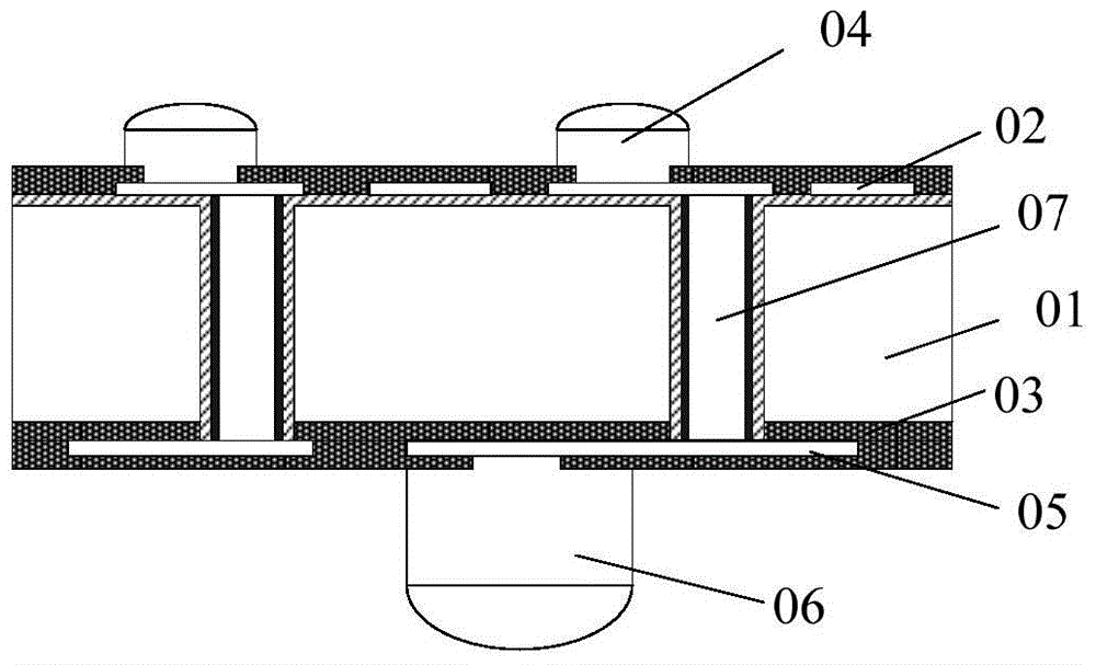
[0168] see Figure 3 (11) , the three-dimensional interconnection structure includes,
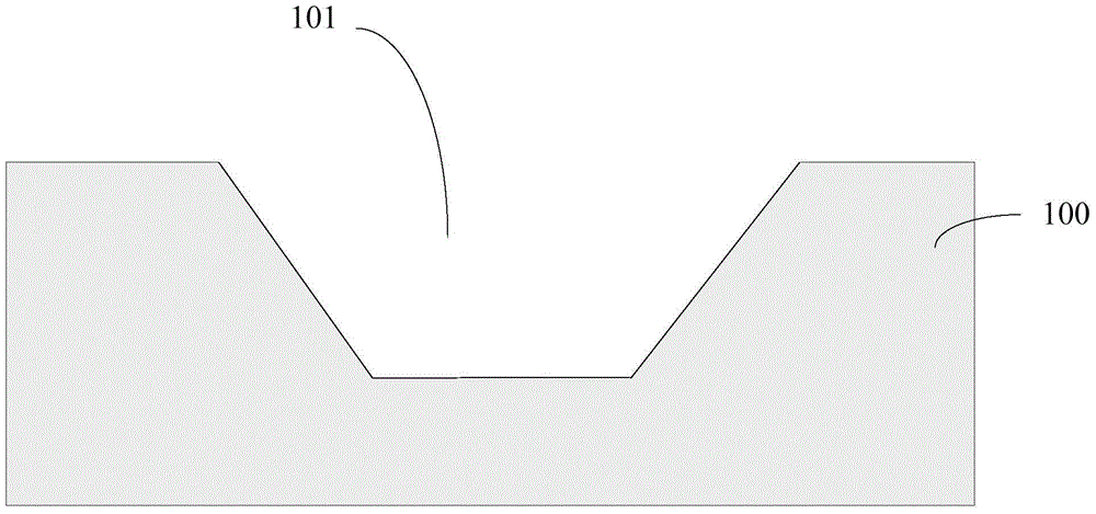
[0169] A semiconductor substrate 100, the semiconductor substrate 100 includes opposite front and back, the semiconductor substrate is formed with a trapezoidal hole 101 through the front and back, the opening of the trapezoidal hole on the front of the semiconductor substrate 100 is larger than an opening on the back side of the semiconductor substrate 100;
[0170] It should be noted that the trapezoidal grooves are formed on the front side of the semiconductor substrate by selective etching, and after the front side process is completed, the thickness of the semiconductor substrate 100 is ground and thinned to form a trapezoidal hole structure.
[0171] The front insulating layer 102 located above the front of the semiconductor substrate 100 and above the slope of the trapezoidal hole 101; since there is no front insulating layer 102 at the bottom of the trapezoidal hole 101, the front ...
PUM
 Abstract
Description
Claims
Application Information
 - R&D
- Intellectual Property
- Life Sciences
- Materials
- Tech Scout
- Unparalleled Data Quality
- Higher Quality Content
- 60% Fewer Hallucinations
Browse by: Latest US Patents, China's latest patents, Technical Efficacy Thesaurus, Application Domain, Technology Topic, Popular Technical Reports.
© 2025 PatSnap. All rights reserved.Legal|Privacy policy|Modern Slavery Act Transparency Statement|Sitemap|About US| Contact US: help@patsnap.com