Horizontal high-voltage super junction power semiconductor device
A power semiconductor and lateral high voltage technology, which is applied in the direction of semiconductor devices, semiconductor/solid-state device manufacturing, electrical components, etc., can solve the problems of N/P charge imbalance of lateral superjunction devices, so as to overcome adverse effects and reduce specific conduction Resistance, the effect of improving the withstand voltage of the device
- Summary
- Abstract
- Description
- Claims
- Application Information
AI Technical Summary
Problems solved by technology
Method used
Image

Examples
Embodiment Construction
[0022] Below in conjunction with accompanying drawing, describe technical scheme of the present invention in detail:
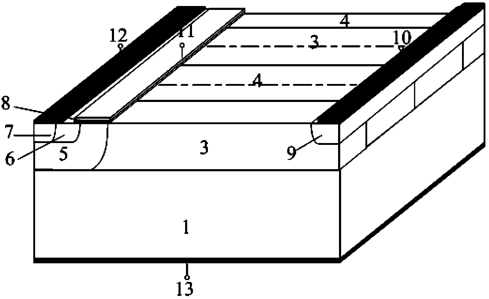
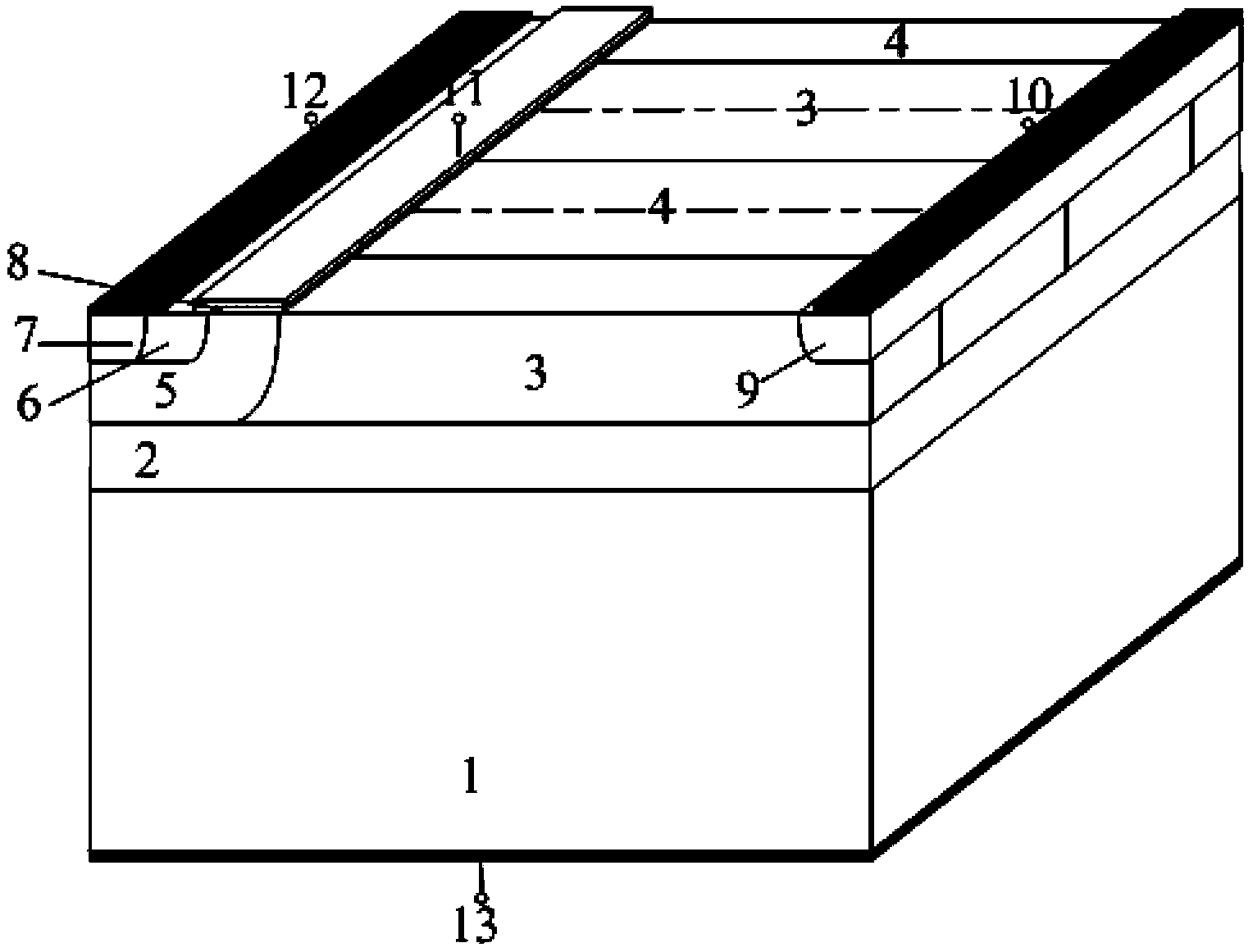
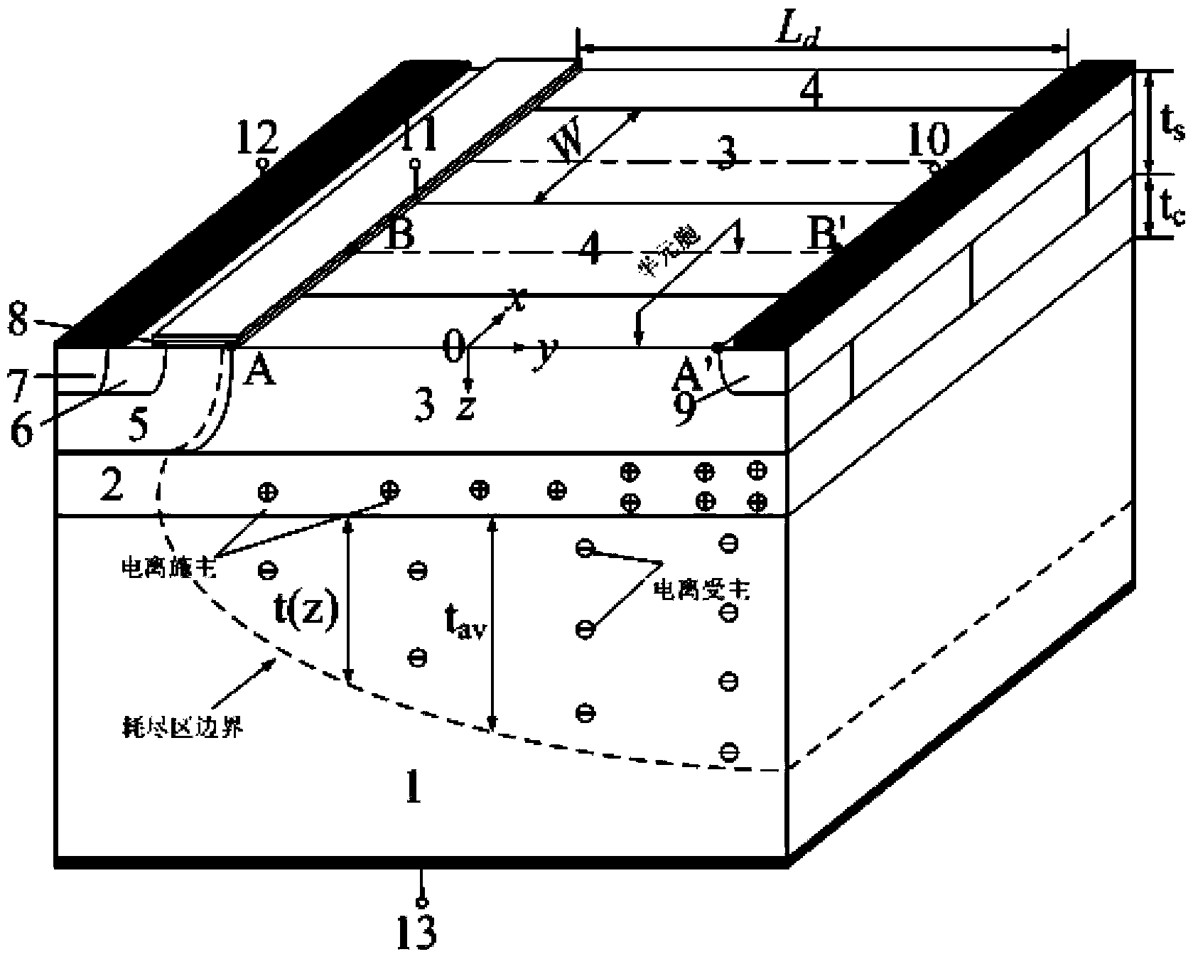
[0023] Such as figure 1 As shown, it is a traditional lateral high-voltage super-junction power semiconductor device, and its cell structure includes a P-type substrate 1, an N-type strip region 3, a P-type strip region 4, a P-type body region 5, and an N-type heavily doped source region. 6. P-type heavily doped region body region 7, gate oxide layer 8, N + The drain region 9, the drain contact electrode 10, the polysilicon gate 11, the source contact electrode 12 and the substrate contact electrode 13; the N-type strip region 3 and the P-type strip region 4 are vertically staggered along the upper surface of the P-type substrate 1 arranged to form a super junction structure, the P-type body region 5 is arranged at one end of the upper surface of the P-type substrate 1 and connected to the super junction structure, and the N + The drain region 9 is arranged ...
PUM
 Abstract
Description
Claims
Application Information
 - R&D
- Intellectual Property
- Life Sciences
- Materials
- Tech Scout
- Unparalleled Data Quality
- Higher Quality Content
- 60% Fewer Hallucinations
Browse by: Latest US Patents, China's latest patents, Technical Efficacy Thesaurus, Application Domain, Technology Topic, Popular Technical Reports.
© 2025 PatSnap. All rights reserved.Legal|Privacy policy|Modern Slavery Act Transparency Statement|Sitemap|About US| Contact US: help@patsnap.com