A gallium nitride-based LED epitaxial structure and preparation method thereof
An epitaxial structure, gallium nitride-based technology, applied in the direction of electrical components, circuits, semiconductor devices, etc., can solve the problems of low luminous efficiency, low yield, poor photoelectric performance, etc., to improve luminous efficiency, improve yield, improve Effect of crystallization quality
- Summary
- Abstract
- Description
- Claims
- Application Information
AI Technical Summary
Problems solved by technology
Method used
Image
Examples
Embodiment 1
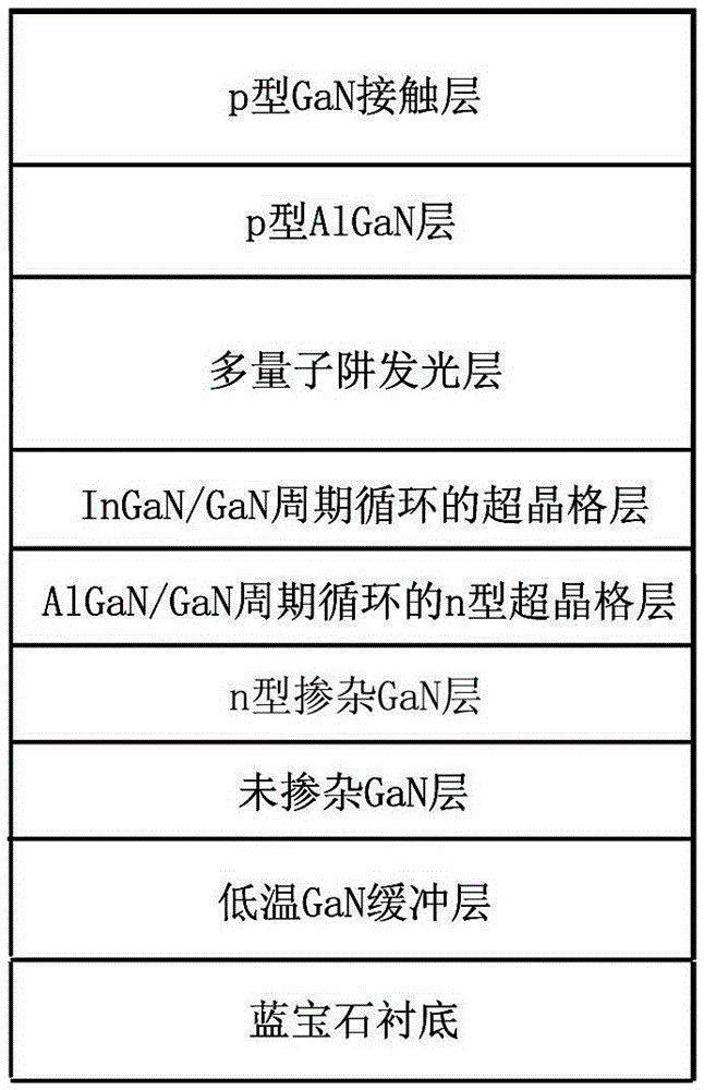
[0019] A GaN-based LED epitaxial structure, including a sapphire substrate, a low-temperature GaN buffer layer, an undoped GaN layer, an n-type doped GaN layer, a superlattice layer, a multi-quantum well light-emitting layer, a p-type AlGaN layer, and a p-type AlGaN layer. Type GaN contact layer; wherein, the low-temperature GaN buffer layer is grown on the upper surface of the sapphire substrate; the undoped GaN layer is grown on the upper surface of the low-temperature GaN buffer layer; the n-type doped GaN layer is grown on the undoped GaN layer surface; the superlattice layer is grown on the upper surface of the n-type doped GaN layer; the multi-quantum well light-emitting layer is grown on the upper surface of the superlattice layer; the p-type AlGaN layer is grown on the upper surface of the multi-quantum well light-emitting layer; the p-type A GaN contact layer is grown on the upper surface of the p-type AlGaN layer.
[0020] In this example, if figure 1 As shown, the ...
Embodiment 2
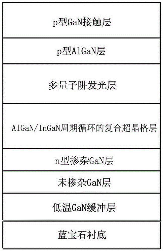
[0035] A GaN-based LED epitaxial structure, including a sapphire substrate, a low-temperature GaN buffer layer, an undoped GaN layer, an n-type doped GaN layer, a superlattice layer, a multi-quantum well light-emitting layer, a p-type AlGaN layer, and a p-type AlGaN layer. Type GaN contact layer; wherein, the low-temperature GaN buffer layer is grown on the upper surface of the sapphire substrate; the undoped GaN layer is grown on the upper surface of the low-temperature GaN buffer layer; the n-type doped GaN layer is grown on the undoped GaN layer surface; the superlattice layer is grown on the upper surface of the n-type doped GaN layer; the multi-quantum well light-emitting layer is grown on the upper surface of the superlattice layer; the p-type AlGaN layer is grown on the upper surface of the multi-quantum well light-emitting layer; the p-type A GaN contact layer is grown on the upper surface of the p-type AlGaN layer.
[0036] In this example, if figure 2 As shown, the...
PUM
 Abstract
Description
Claims
Application Information

