AZO thin film, preparing method and MEMS device comprising AZO thin film

A thin film and device technology, which is applied in the field of transparent conductive thin films, can solve the problems of expensive ITO thin film manufacturing, difficult chemical vapor deposition, and lattice matching of the thin film phase, and achieve low cost, good lattice matching, and good lattice matching. Effect

Active Publication Date: 2014-01-15
CSMC TECH FAB2 CO LTD
View PDF5 Cites 11 Cited by
  • Summary
  • Abstract
  • Description
  • Claims
  • Application Information

AI Technical Summary

Problems solved by technology

However, ITO thin films have disadvantages such as expensive manufacturing costs, toxic raw materials used, and great environmental hazards.
And in MEMS devices, it is usually necessary to deposit and form other dielectric films on the ITO film, and it is usually difficult to form a chemical vapor deposition (CVD) film on the ITO film, because the ITO film is difficult to lattice-matched with the film formed by CVD. of

Method used


Image

  • AZO thin film, preparing method and MEMS device comprising AZO thin film
  • AZO thin film, preparing method and MEMS device comprising AZO thin film
  • AZO thin film, preparing method and MEMS device comprising AZO thin film

Examples


Embodiment Construction

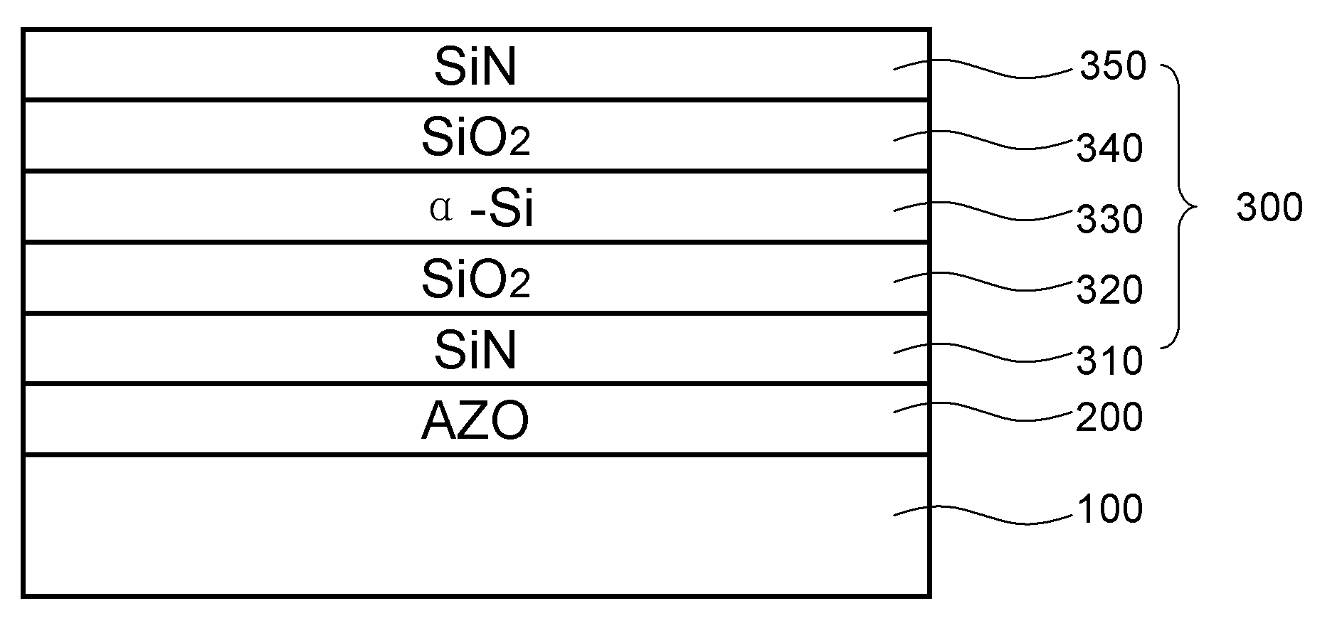
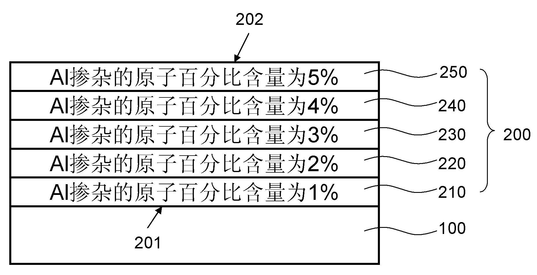
[0031] The following introduces some of the possible embodiments of the present invention, which are intended to provide a basic understanding of the present invention, but are not intended to identify key or decisive elements of the present invention or limit the scope of protection. It is easy to understand that, according to the technical solution of the present invention, those skilled in the art may propose other alternative implementation manners without changing the essence and spirit of the present invention. Therefore, the following specific embodiments and drawings are only exemplary descriptions of the technical solution of the present invention, and should not be regarded as the entirety of the present invention or as a limitation or restriction on the technical solution of the present invention. In the drawings, the thicknesses of layers and regions are exaggerated for clarity.

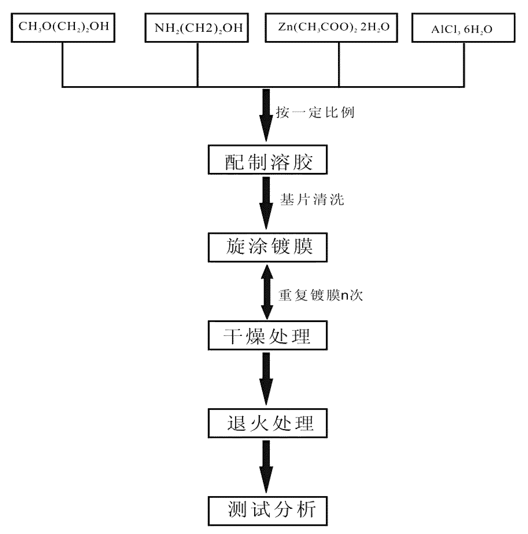
[0032] The applicant noticed that, as a newly proposed wide bandgap semiconductor fil...


PUM


Abstract

An aluminum-doped zinc oxide (AZO) thin film (200), a preparation method thereof, and a micro electro mechanical system (MEMS) device comprising same. The AZO thin film (200) is formed on a substrate (100), the aluminum dosage concentration of the AZO thin film (200) being increased gradually in the thin film thickness direction; in the preparation method, the AZO thin film (200) is prepared by using a sol-gel method; the MEMS device uses the AZO thin film (200) and form a composite thin film layer (300) on the AZO thin film (200) through chemical vapor deposition filming. The AZO thin film (200) has desirable conductivity, has good lattice matching with the composite thin film layer (300), has matched thermal expansion and low cost, and is nontoxic, pollution free, and simple in preparation.

Description

technical field [0001] The invention belongs to the technical field of transparent conductive thin films, and relates to an AZO (aluminum-doped zinc oxide) thin film with a gradient film structure, a preparation method and a MEMS (Micro-Electro-Mechanical System, micro-electromechanical system) device using the AZO thin film. Background technique [0002] Transparent conductive films are widely used in solar cells, MEMS devices, display devices and other fields. For example, in MEMS devices, the preparation of transparent conductive films is an important step in the manufacturing process. [0003] Traditionally, the transparent conductive film commonly used in MEMS devices is an ITO (Indium Tin Oxide, indium tin metal oxide) film. However, ITO thin films have disadvantages such as expensive manufacturing costs, toxic raw materials used, and great harm to the environment. And in MEMS devices, it is usually necessary to deposit and form other dielectric films on the ITO film,...

Claims


Application Information

Patent Timeline
Patent Type & Authority Applications(China)
IPC IPC(8): B81B7/00B81C1/00C23C26/00C23C14/35C23C14/06
CPCC23C14/086C23C16/407H01L21/02554H01L21/02576H01L21/02628
Inventor 谢岩李展信
Owner CSMC TECH FAB2 CO LTD
Why Eureka
Try Eureka