Method of forming FinFET gate medium layer and method of forming FinFET

A gate dielectric layer and transition layer technology, applied in electrical components, semiconductor/solid-state device manufacturing, semiconductor devices, etc., can solve the problems of surface roughness and lattice mismatch of semiconductor fins, and avoid charge trapping, roughness, etc. The effect of reducing the temperature and improving the performance

Active Publication Date: 2014-01-15
SEMICON MFG INT (SHANGHAI) CORP
View PDF4 Cites 16 Cited by
  • Summary
  • Abstract
  • Description
  • Claims
  • Application Information

AI Technical Summary

Problems solved by technology

[0007] In view of this, the present invention provides a method for forming a FinFET gate dielectric layer and a method for forming a FinFET to solve the lattice mismatch between the gate dielectric layer and the semiconductor fin in the prior art, and the surface of the semiconductor fin rough question

Method used


Image

  • Method of forming FinFET gate medium layer and method of forming FinFET
  • Method of forming FinFET gate medium layer and method of forming FinFET
  • Method of forming FinFET gate medium layer and method of forming FinFET

Examples


Embodiment Construction

[0032] In order to describe the principles and features of the present invention in conjunction with the accompanying drawings, the examples given are only used to explain the present invention, not to limit the scope of the present invention.

[0033] Such as figure 2 A method of forming a FinFET gate dielectric layer of the present invention shown, comprising:

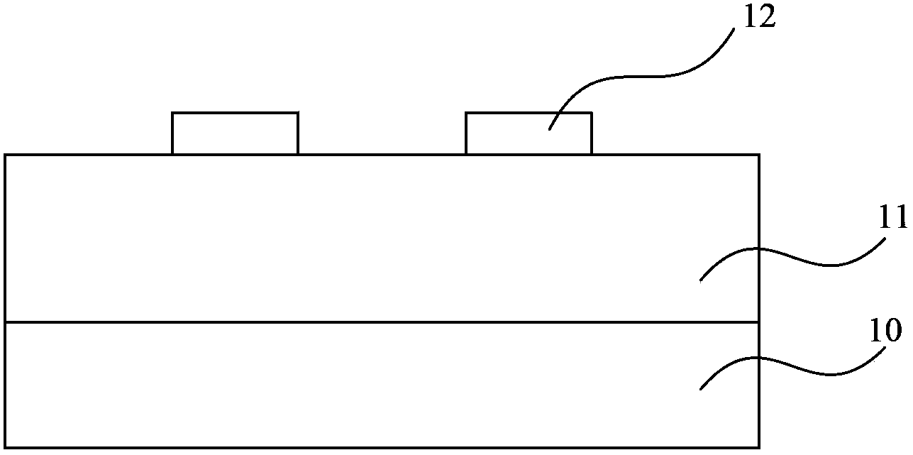
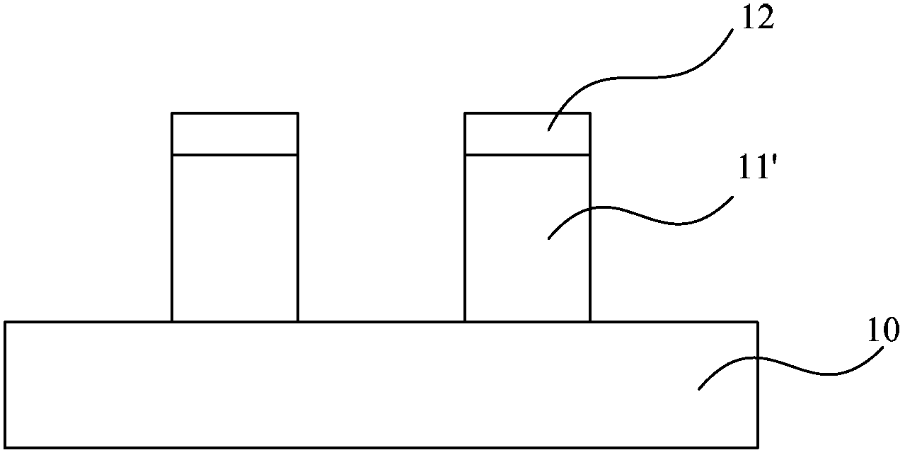
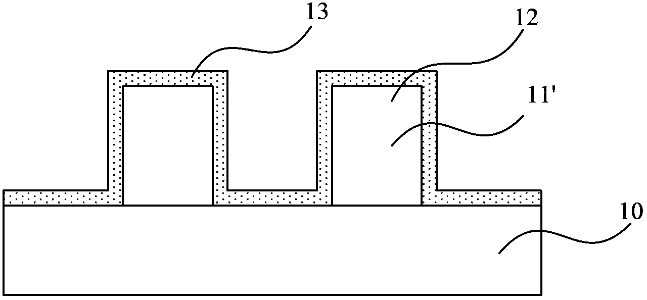
[0034] providing a semiconductor substrate formed with semiconductor fins;

[0035] Epitaxially growing a single crystal silicon layer on the surface of the semiconductor fin, and annealing the semiconductor substrate in a mixed gas atmosphere of deuterium and an inert gas, so as to form a transition layer on the surface of the semiconductor fin;

[0036] A gate dielectric layer is formed on the surface of the semiconductor substrate and the transition layer.

[0037] In order to specifically illustrate the mechanism of the present invention, as a typical embodiment of a method for forming a FinFET disclosed in th...


PUM


Abstract

The invention discloses a method of forming a FinFET gate medium layer and a method of forming a FinFET. After monocrystal silicon is formed in an epitaxial manner on the surface of a semiconductor fin object, and a semiconductor substrate is annealed under a condition of mixed gas including deuterium and inert gas so that a transition layer is obtained. Therefore, problems of crystal lattice mismatch between a gate medium layer and the semiconductor fin object are solved. Moreover, the surface of the semiconductor fin object is reduced in roughness, a charge trapping center is prevented from forming, and then the performance of a semiconductor device is improved.

Description

technical field [0001] The present invention relates to the technical field of semiconductor manufacturing, and in particular to a method for forming a gate dielectric layer of a FinFET (FinField-effect transistor, Fin Field Effect Transistor) and a method for forming a FinFET. Background technique [0002] With the development of semiconductor technology, the feature size of metal oxide semiconductor transistor (MOSFET), which is one of the signs of its development, has been continuously shrinking following Moore's law. In order to meet the miniaturization and high performance requirements of integrated circuits, three-dimensional integration technology has been widely valued in recent years. Taking MOS as an example, three-dimensional structures such as horizontal multi-faceted gate structure and vertical multi-faceted gate structure have been developed. [0003] The three-dimensional multi-plane gate MOSFET can be intuitively divided into horizontal multi-plane gate MOSFE...

Claims


Application Information

Patent Timeline
Patent Type & Authority Applications(China)
IPC IPC(8): H01L21/28H01L21/336
CPCH01L21/28158H01L21/28185H01L29/66795
Inventor 赵猛
Owner SEMICON MFG INT (SHANGHAI) CORP
Why Eureka
Try Eureka