Production method of semiconductor device

A device manufacturing method and semiconductor technology, applied in the direction of semiconductor/solid device manufacturing, semiconductor devices, electrical components, etc., can solve the problems of increasing corrosion rate, increasing defects, prolonging corrosion time, etc., to reduce roughness, reduce Defects, the effect of improving device performance

Active Publication Date: 2014-01-29
INST OF MICROELECTRONICS CHINESE ACAD OF SCI
View PDF4 Cites 9 Cited by
  • Summary
  • Abstract
  • Description
  • Claims
  • Application Information

AI Technical Summary

Problems solved by technology

[0007] However, in the above existing processes, due to the relatively large distance a1, the SiGe and/or SiC stress source and drain regions have to go through a long distance to apply stress to the channel region, and the actual increase in stress obtained by the channel region is limited.
In addition, if a1 is increased

Method used


Image

  • Production method of semiconductor device
  • Production method of semiconductor device
  • Production method of semiconductor device

Examples


Embodiment Construction

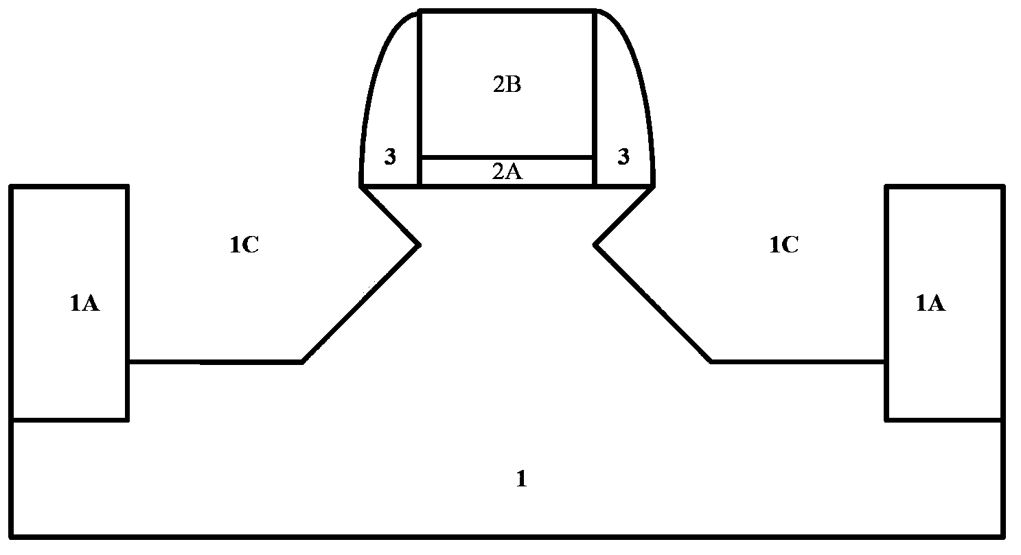
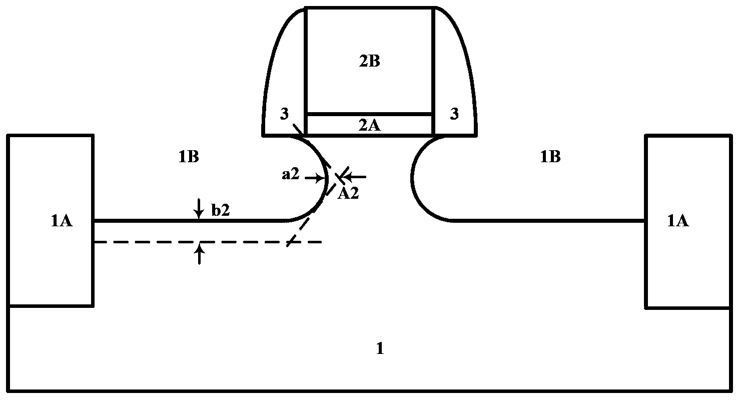
[0024] The features and technical effects of the technical solutions of the present invention will be described in detail below with reference to the accompanying drawings and in conjunction with the schematic embodiments. It should be noted that similar reference numerals denote similar structures, and the terms "first", "second", "upper", "lower", "thick", "thin", etc. used in this application may be used for Trim various device structures. These modifications do not imply a spatial, sequential, or hierarchical relationship of the modified device structures unless specifically stated.

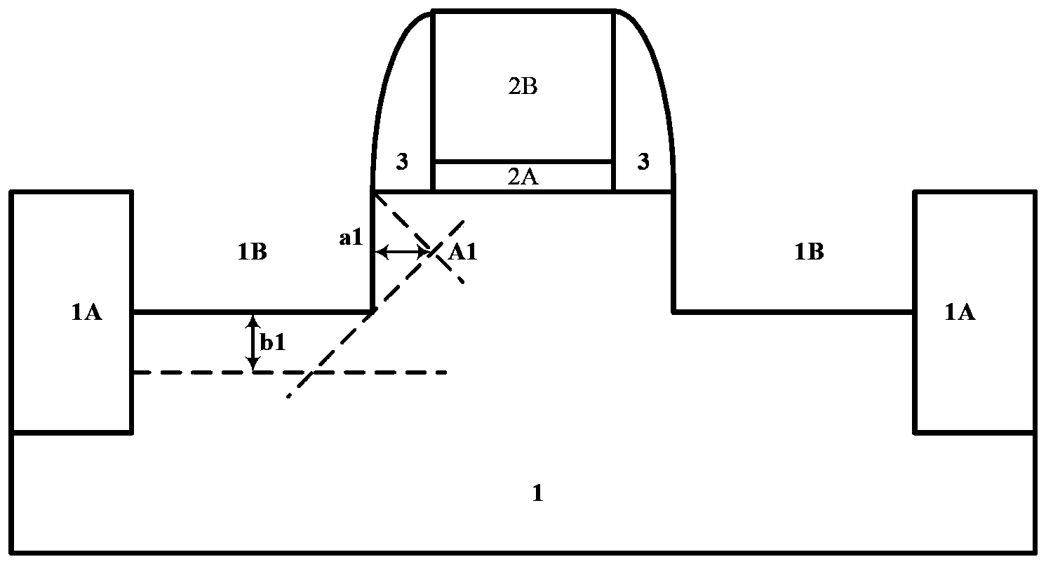
[0025] refer to Figure 5 as well as image 3 , dry etching the substrate to form C-type source and drain grooves.

[0026] Provide a substrate 1, provide a substrate 1, which can be bulk Si, SOI, bulk Ge, GeOl, SiGe, GeSb, or a III-V or II-VI compound semiconductor substrate, such as GaAs, GaN, InP , InSb, etc. In order to be compatible with the existing CMOS process for application in ...


PUM


Abstract

The invention discloses a production method of a semiconductor device. The production method includes: forming a gate stack structure on a substrate; etching parts of the substrate, on two sides of the gate stack structure, to form C-shaped source-drain trenches; wet-etching the C-shaped source-drain trenches to form sigma-shaped source-drain trenches. According to the production method of the semiconductor device, the C-shaped source-drain trenches are etched and sigma-shaped source-drain trenches are formed by further wet etching; accordingly, channel area stress is increased effectively, the depth of source-drain trenches is controlled precisely, defects are reduced, the sidewall and bottom of each trench is less rough, and the performance of the device is improved.

Description

technical field [0001] The invention relates to the field of manufacturing semiconductor integrated circuits, and more specifically, to a semiconductor device method with Σ-type source and drain. Background technique [0002] After entering the 90nm node, strained silicon technology has become a basic technology to improve the performance of MOSFET devices by suppressing the short channel effect and improving carrier mobility. In the strained silicon technology, stress technologies such as STI, SPT, source-drain silicon germanium embedding, metal gate stress, etch stop layer (CESL) have been proposed successively, and various schemes are used to apply stress to the channel region to increase the current carrying capacity. sub-mobility to improve actuation. [0003] Among these technologies, the source-drain silicon-germanium embedded technology is gradually adopted by mainstream CMOS process manufacturers after entering the 90nm node. The method of epitaxially growing silic...

Claims


Application Information

Patent Timeline
IPC IPC(8): H01L21/336
CPCH01L29/7848H01L29/66636H01L21/30604H01L21/26506H01L29/66477H01L21/30608H01L21/3065
Inventor 秦长亮洪培真殷华湘
Owner INST OF MICROELECTRONICS CHINESE ACAD OF SCI
Why Eureka
Try Eureka