
Testing method and device of LVDS (low voltage differential signaling) interface of SOC (system on chip)

A technology of interface testing and chips, which is applied in the direction of frequency measurement devices, detecting faulty computer hardware, etc., can solve the problems of complex logic code and test vector writing, high test platform price, low test efficiency, etc., to reduce test cost, Inexpensive, easy-to-write effects

Inactive Publication Date: 2014-02-05
ALLWINNER TECH CO LTD
View PDF4 Cites 6 Cited by
  • Summary
  • Abstract
  • Description
  • Claims
  • Application Information

AI Technical Summary

Problems solved by technology

The test platform is expensive and usually costs more than hundreds of thousands of yuan, resulting in high test costs; at the same time, the writing of logic codes and test vectors is relatively complicated, so the test efficiency is low

Method used


Image

  • Testing method and device of LVDS (low voltage differential signaling) interface of SOC (system on chip)
  • Testing method and device of LVDS (low voltage differential signaling) interface of SOC (system on chip)
  • Testing method and device of LVDS (low voltage differential signaling) interface of SOC (system on chip)

Examples


Embodiment Construction

[0045] The present invention will be further described below in conjunction with the accompanying drawings and specific embodiments.

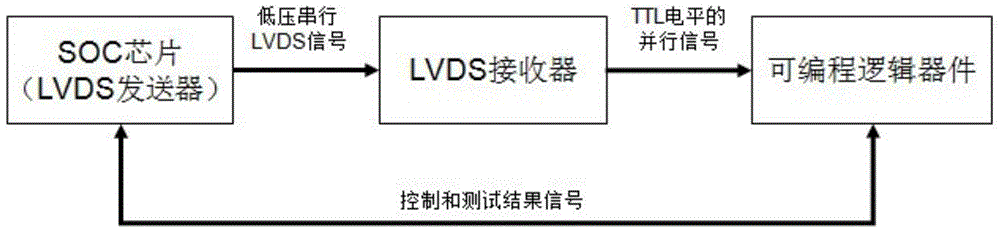
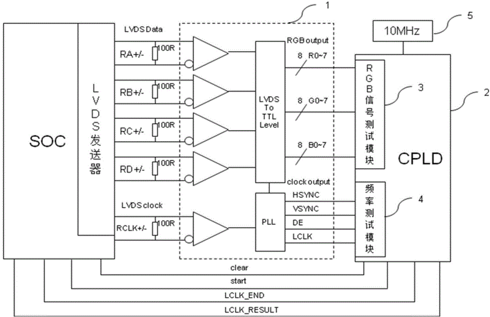
[0046] Such as figure 1 , figure 2 As shown, the SOC chip LVDS interface test device includes an LVDS receiver 1 and a programmable logic device 2, and the programmable logic device 2 can use CPLD (Complex Programmable Logic Device) or FPGA (Field-Programmable Gate Array). The LVDS receiver 1 converts the LVDS serial signal output by the LVDS transmitter integrated in the SOC chip into a TTL level parallel signal, and then tests the TTL level parallel signal through the programmable logic device 2. After the test is completed, the The SOC chip returns the test result.

[0047] The parallel signal of TTL level includes 24bit RGB signal and 4 channels of frequency signal, of which 24bit RGB signal includes R0~7, G0~7, B0~7, and 4 channels of frequency signal include main frequency signal LCLK, line synchronization signal HSYNC, field synchroni...


PUM


Abstract

The invention relates to the technical field of LVDS (low voltage differential signaling) interfaces, and provides a testing method of an LVDS interface of an SOC (system on chip). The testing method comprises the steps of converting a serial signal output by an LVDS transmitter integrated in the SOC into a parallel signal of a TTL level, and then testing the parallel signal of the TTL level. The invention also provides a testing device of the LVDS interface of the SOC. The testing device comprises an LVDS receiver used for converting the serial signal output by the LVDS transmitter integrated in the SOC into the parallel signal of the TTL level, and a programmable logic device used for testing the parallel signal of the TTL level. The testing device provided by the invention is low in price, and has obvious price advantage compared with the existing ATE (automatic test equipment) testing platform, and the testing cost is greatly reduced.

Description

technical field [0001] The invention relates to the technical field of LVDS interfaces, in particular to a testing method for an LVDS interface integrated in an SOC chip. Background technique [0002] LVDS (Low Voltage Differential Signaling) interface is a low-voltage differential signal interface, which uses a very low voltage swing to transmit data through differential transmission on two PCB traces or a pair of balanced cables, with high speed, low noise, and low power consumption. Power consumption and other characteristics, widely used in various consumer electronics such as pad, mp4, navigator and other products in the display. The LVDS interface circuit includes two parts: the LVDS output interface circuit on the driver board side, that is, the LVDS transmitter, and the LVDS input interface circuit on the liquid crystal panel side, that is, the LVDS receiver. [0003] With the development of system integration technology, various consumer electronics are currently u...

Claims


Application Information

Patent Timeline
IPC IPC(8): G06F11/22G01R23/02
Inventor 钟汝军陈荣志杜联平
Owner ALLWINNER TECH CO LTD
Learn More