Chemical vapor deposition equipment used for producing silicon carbide epitaxial wafer

A technology of chemical vapor deposition and epitaxial wafers, which is applied in the direction of chemically reactive gases, chemical instruments and methods, and single crystal growth, which can solve problems such as uniformity and surface defects, thick silicon carbide epitaxial layers, and increased manufacturing costs. Achieve the effects of simple cost input, reduced thickness difference, and small uniformity

Active Publication Date: 2014-02-26
GLOBAL ENERGY INTERCONNECTION RES INST CO LTD +2
View PDF3 Cites 6 Cited by
  • Summary
  • Abstract
  • Description
  • Claims
  • Application Information

AI Technical Summary

Problems solved by technology

[0004] The patent number is ZL98812328.2, and the patent titled "Growing very uniform silicon carbide epitaxial layer" discloses an improved chemical vapor deposition method. The reactor is heated until the silicon carbide raw material gas forms an epitaxial layer on the substrate in the reactor. The temperature of the raw material gas and the carrier gas flow through the heated reactor to form a silicon carbide epitaxial layer on the substrate. At the same time, the carrier gas includes a mixture of hydrogen and a second gas, wherein the thermal conductivity of the second gas is lower than that of hydrogen. lead, so that the consumption of the raw materi

Method used


Image

  • Chemical vapor deposition equipment used for producing silicon carbide epitaxial wafer
  • Chemical vapor deposition equipment used for producing silicon carbide epitaxial wafer
  • Chemical vapor deposition equipment used for producing silicon carbide epitaxial wafer

Examples


Embodiment 1

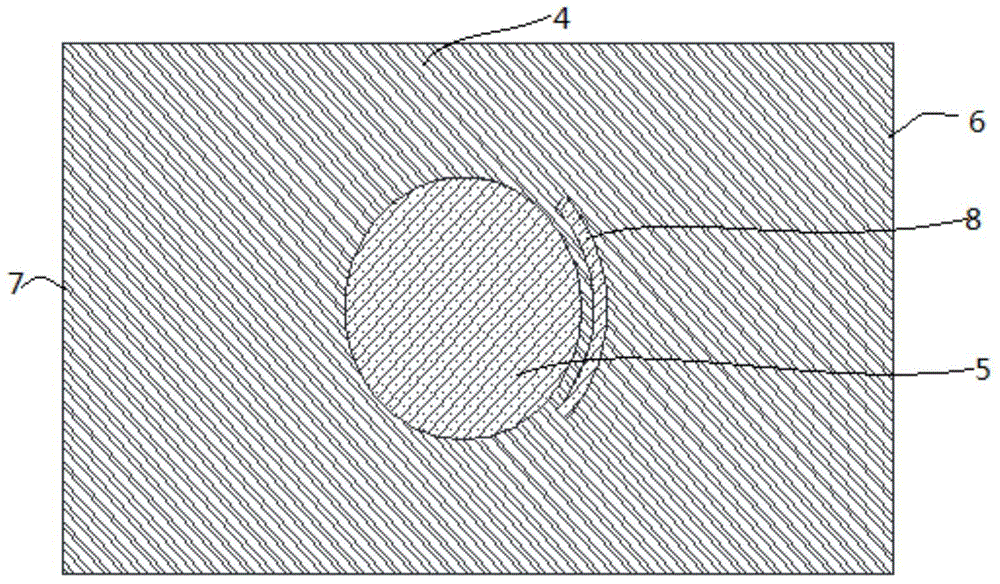
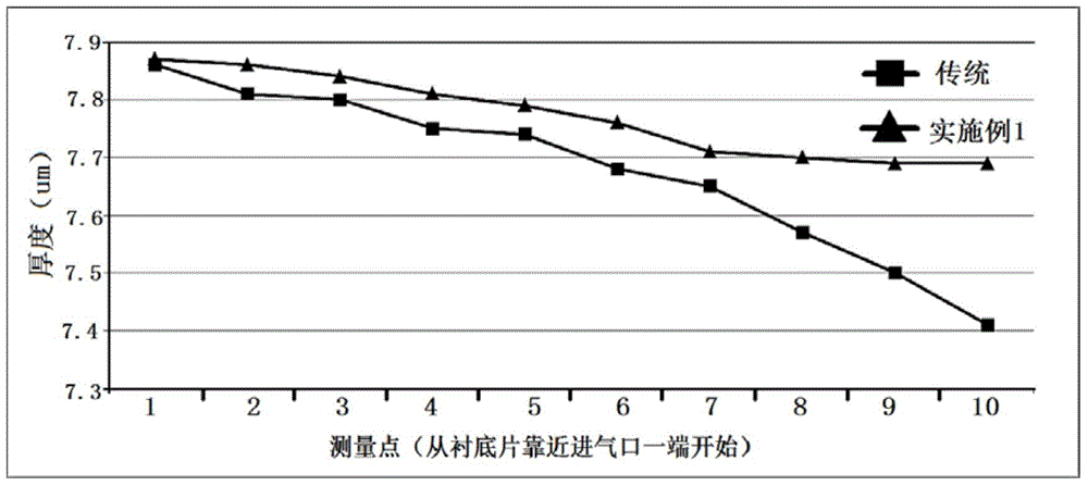
[0028] Such as image 3 As shown, the arc of the barrier ring is 180 degrees, the width is 0.9 cm, and the setting height is 0.4 cm. Through the above process, the growth of the epitaxial wafer is completed. In the direction of the corresponding airflow of the silicon carbide substrate, 10 points are measured at intervals, point 1 corresponds to the upper part of the airflow, and point 10 corresponds to the lower part of the airflow. The measurement results are as follows: Figure 5 As shown, the thickness of the silicon carbide epitaxial wafer obtained in Example 1 is reduced from 2.13% to 0.97%.

Embodiment 2

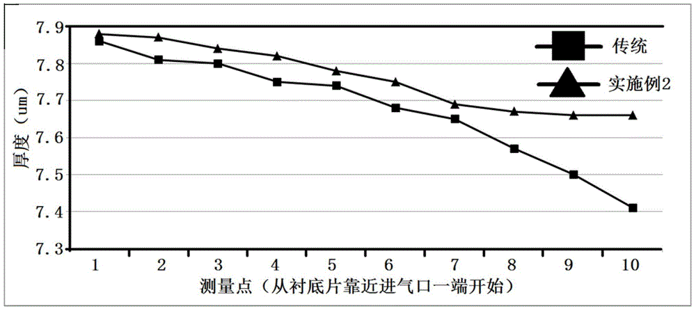
[0030] Such as Figure 4 As shown, when the arc of the barrier ring is 90 degrees, the width is 1.0 cm, and the height is set to 0.5 cm, the growth of the epitaxial wafer is completed through the above process flow. In the direction of the corresponding airflow of the silicon carbide substrate, 10 points are measured at intervals, point 1 corresponds to the upper part of the airflow, and point 10 corresponds to the lower part of the airflow. The measurement results are as follows: Image 6 As shown, the thickness uniformity of the silicon carbide epitaxial wafer obtained in Example 2 is reduced from 2.13% to 1.19%.

Embodiment 3

[0032] The width of the graphite barrier ring is 0.8cm, the height is 0.3cm, the radius is 1cm larger than the width of the substrate wafer, and the thickness uniformity of the epitaxial wafer prepared when the radian is 100 degrees is reduced from 2.16% to 1.21%.


PUM

PropertyMeasurementUnit
Radianaaaaaaaaaa
Radianaaaaaaaaaa

Abstract

The invention provides a method for improving the uniformity of silicon carbide epitaxial wafer, and the method can be used to produce silicon carbide epitaxial wafers with an even thickness. The method comprises the following steps: installing an air flow blocking ring under the air flow of a reaction cavity, then placing a silicon carbide substrate on a supporting platform, heating the reaction cavity to a temperature required by the epitaxy, and introducing reaction gas and carrier gas so as to finally form a silicon carbide epitaxial layer on the silicon carbide substrate. The silicon carbide epitaxial wafer obtained by the method has a more even thickness, besides the equipment is simple, so the method is a most practicable and cheapest method for improving conventional equipment, does not need much investment, and is benefit for the industrial production.

Description

【Technical Field】 [0001] The invention belongs to the field of chemical vapor deposition, and specifically relates to a chemical vapor deposition equipment for producing silicon carbide epitaxial wafers. 【Background technique】 [0002] Silicon carbide (SiC) is the third-generation wide-bandgap semiconductor material. It has the characteristics of wide band gap, high critical breakdown electric field, high thermal conductivity, and high carrier saturation drift speed. It is especially suitable for the production of high-temperature, high-voltage, high-power power electronics Such semiconductor devices are of great significance to the development of industries such as hybrid electric vehicles, electric vehicles, solar inverters, and smart grids. [0003] The production of silicon carbide materials is not easy, whether it is crystal growth or epitaxial growth. Growing high-quality epitaxial wafers is a challenge to the process. The traditional chemical vapor deposition method to grow...

Claims


Application Information

Patent Timeline
IPC IPC(8): C30B29/36C30B25/20C30B25/10C30B25/14
Inventor 钮应喜杨霏于坤山
Owner GLOBAL ENERGY INTERCONNECTION RES INST CO LTD
Why Eureka
Try Eureka