A silicon carbide epitaxial growth device

A technology of epitaxial growth and silicon carbide, which is applied in the direction of single crystal growth, crystal growth, single crystal growth, etc., can solve the problems of increasing manufacturing costs, polluting epitaxial wafers, and large environmental pollution, and achieves improved uniformity, increased growth rate, and The effect of increasing the growth rate

Active Publication Date: 2016-04-20
GLOBAL ENERGY INTERCONNECTION RES INST CO LTD +2
View PDF3 Cites 0 Cited by
  • Summary
  • Abstract
  • Description
  • Claims
  • Application Information

AI Technical Summary

Problems solved by technology

[0006] High-voltage silicon carbide power electronic devices require an epitaxial layer thickness of tens of microns to hundreds of microns, and a device with a general voltage of 10kV requires an epitaxial thickness of about 100um, while the current mature silicon carbide epitaxial growth rate is only about 5-7um / h , if a 100um thick silicon carbide epitaxial material is grown at such a growth rate, it will take 14-20 hours, which obviously greatly increases the manufacturing cost, and with the extension of the epitaxial growth cycle, more pollutants will be deposited on the reaction chamber wall , and then pollute the epitaxial wafer, so in order to grow high-quality, thick silicon carbide epitaxial wafers, the growth rate of epitaxy must be increased
[0007] The possible reason for the slow growth rate is that the decomposition rate of the reaction source gas is low and the easily formed silicon aggregates in the reaction gas. How to increase the growth rate is to improve the decomposition rate of the reaction source or suppress the generation of silicon aggregates. In the prior art , by introducing Cl compounds into the reaction gas flow, the etching effect of Cl elements is used to inhibit the formation of silicon aggregates, so as to increase the growth rate, but the introduction of Cl compounds requires additional gas pipelines and other equipment, and contains Cl The tail gas of the elements is extremely polluting to the environment

Method used


Image

  • A silicon carbide epitaxial growth device

Examples


Embodiment 1

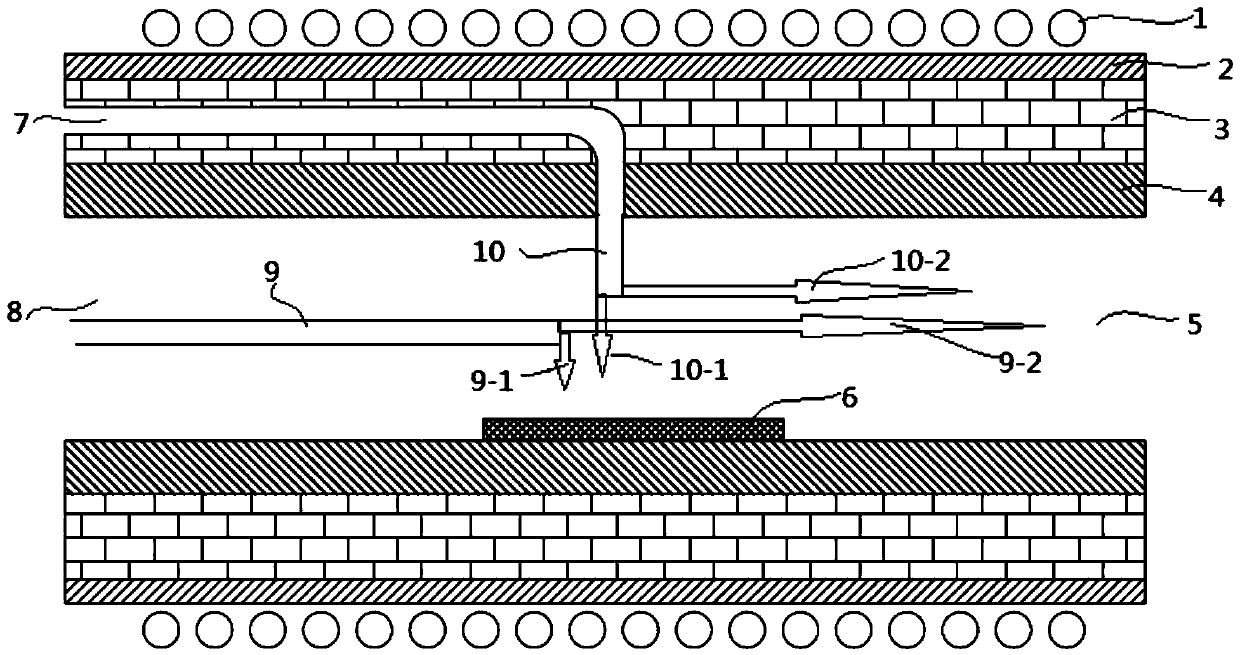
[0069] Such as figure 1 As shown, a silicon carbide epitaxial growth device of the present invention has a cylindrical shape and a cross-sectional radius of 18 cm, wherein a heating coil, a quartz wall, a graphite soft felt, a graphite support layer and the surrounding parts are arranged sequentially from the outside to the inside. Cuboid reaction chamber, the two ends of the reaction chamber are respectively equipped with an air inlet device and an air outlet device, the inner wall of the graphite support layer is coated with a coating, the coating is silicon carbide, and the thickness is 70um. Felt and vertically pass through the L-shaped air supply pipe of the graphite support layer, and the inner wall of the air supply pipe is coated with a coating.

[0070] The thickness of the quartz wall is 4 mm, and the thickness of the graphite support layer is 1.5 cm.

[0071] The gas supply pipes side by side covering the entire section of the reaction chamber are made of high-puri...

Embodiment 2

[0080] Such as figure 1 As shown, a kind of silicon carbide epitaxial growth device of the present invention, device is cylindrical, and cross-sectional radius is 20cm, wherein is provided with heating coil, quartz wall, graphite soft felt, graphite support layer and surrounded by it successively from outside to inside Cuboid reaction chamber, the two ends of the reaction chamber are respectively equipped with an air inlet device and an air outlet device, the inner wall of the graphite support layer is coated with tantalum carbide, and the thickness is 80um. Felt and vertically pass through the L-shaped air supply pipe of the graphite support layer, and the inner wall of the air supply pipe is coated with a coating.

[0081] The thickness of the quartz wall is 5 mm, and the thickness of the graphite support layer is 1.8 cm.

[0082] The gas supply pipes side by side covering the entire section of the reaction chamber are made of high-purity graphite, and the inner wall is coa...

Embodiment 3

[0091] Such as figure 1 As shown, a kind of silicon carbide epitaxial growth device of the present invention, device is cylindrical, and cross-sectional radius is 25cm, wherein is provided with heating coil, quartz wall, soft graphite felt, graphite support layer and surrounded by it successively from outside to inside Cuboid reaction chamber, the two ends of the reaction chamber are respectively equipped with an air inlet device and an air outlet device, the inner wall of the graphite support layer is coated with silicon carbide, and the thickness is 90um. Felt and vertically pass through the L-shaped air supply pipe of the graphite support layer, and the inner wall of the air supply pipe is coated with a coating.

[0092] The thickness of the quartz wall is 6 mm, and the thickness of the graphite support layer is 2.0 cm.

[0093] The air supply pipes covering the entire section of the reaction chamber side by side are made of high-purity graphite, and the inner wall is coat...


PUM

PropertyMeasurementUnit
diameteraaaaaaaaaa
radiusaaaaaaaaaa
thicknessaaaaaaaaaa

Abstract

The invention provides a device for epitaxial growth of silicon carbide. The cylindrical device is sequentially provided with a heating coil, a quartz wall, a graphite soft felt, a graphite support layer and a reaction cavity surrounded by the graphite support layer from outside to inside, wherein a gas inlet device and a gas outlet device are respectively arranged at two ends of the reaction cavity, a clad layer is plated on the inner wall of the graphite support layer, L-shaped gas supplementing tubes which are arranged side by side are parallel to the cylindrical device in axial direction, pass through the graphite soft felt and vertically pass through the graphite support layer, and clad layers are plated on the inner walls of the gas supplementing tubes. The gas provided by the gas supplementing tubes of the device compensates the lower part of the gas flow, so that the concentrations of the upper part and the lower part of the gas flow are generally the same, and the uniformity of the thickness of an epitaxial layer of silicon carbide is improved; gas phase nucleation in gas is inhibited, the growth rate is improved, and ultra thick silicon carbide epitaxial wafers with uniform height can be rapidly prepared. The device has a simple structure, is simple to manufacture and implement, has low manufacture cost, is easy to install and operate, and is applicable to industrial production; the epitaxial growth rate is high, and the quality of silicon carbide is good.

Description

technical field [0001] The invention relates to a crystal epitaxial layer growth device, in particular to a silicon carbide epitaxial growth device. Background technique [0002] Silicon carbide (SiC) is the third-generation semiconductor material developed after the first-generation semiconductor materials silicon, germanium and the second-band semiconductor materials gallium arsenide and indium phosphide. The wide bandgap of silicon carbide materials is silicon and arsenide 2 to 3 times that of gallium, so that semiconductor devices can work at a relatively high temperature (above 500 ° C) and have the ability to emit blue light; the high breakdown electric field is an order of magnitude higher than that of silicon and gallium arsenide, which determines the semiconductor device. Excellent high-voltage and high-power performance; high saturated electron drift velocity and low dielectric constant determine the high-frequency and high-speed operating performance of the device...

Claims


Application Information

Patent Timeline
Patent Type & Authority Patents(China)
IPC IPC(8): C30B25/14C30B29/36
Inventor 钮应喜杨霏于坤山
Owner GLOBAL ENERGY INTERCONNECTION RES INST CO LTD
Why Eureka
Try Eureka