N-polarity InGaN-based solar cell based on ScAlN and InAlN polarization insertion layer enhanced electric field

A solar cell and intercalation layer technology, applied in the field of microelectronics, can solve the problems of InGaN material epitaxy is difficult and the difference in spontaneous polarization is not large, so as to reduce the impact of epitaxial growth, enhance drift ability, and ensure crystal quality.

Active Publication Date: 2020-10-16
XIDIAN UNIV
View PDF14 Cites 1 Cited by
  • Summary
  • Abstract
  • Description
  • Claims
  • Application Information

AI Technical Summary

Problems solved by technology

In order to solve this problem, it was proposed to use the N polar structure, so that the polarization electric field can be used to assist in enhancing the drift electric field, thereby enhancing the drift ability of photogenerated carriers, but due to the spontaneous polarization between GaN and InGaN ternary alloys The difference itself is not big. It is difficult to form a large polarization electric field only by the piezoelectric polarization difference between the InGaN alloy material and GaN. In addition, the epitaxy of the high In composition InGaN material is difficult, so only relying on the N polarity structure to enhance the drift ability of photogenerated carriers in InGaN-based solar cells has little effect

Method used


Image

  • N-polarity InGaN-based solar cell based on ScAlN and InAlN polarization insertion layer enhanced electric field
  • N-polarity InGaN-based solar cell based on ScAlN and InAlN polarization insertion layer enhanced electric field

Examples


Embodiment 1

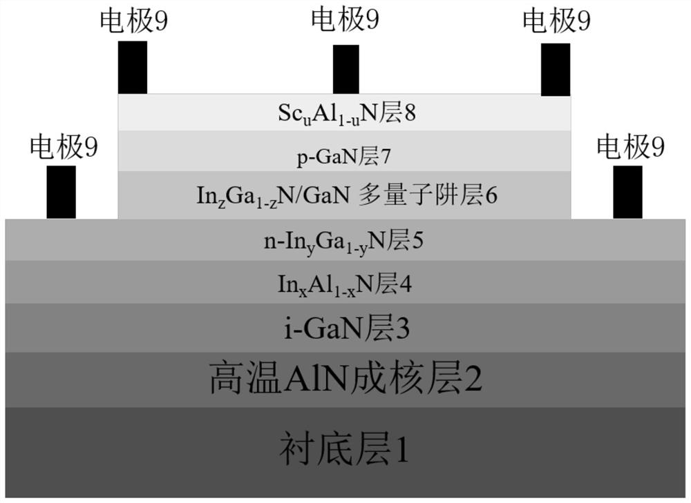
[0039] Example 1, preparing In on a SiC substrate with a thickness of 10nm 0.21 al 0.79 N-polarization enhancement layer and Sc with a thickness of 10nm 0.3 al 0.7 N-polarized enhancement layer, 30 cycles of In 0.15 Ga 0.85 N / GaN multiple quantum wells, N-polar InGaN-based solar cells that can absorb 420nm light wavelength.

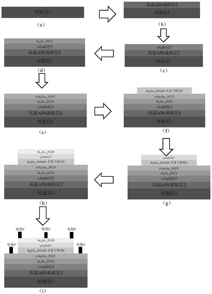
[0040] In step one, the substrate is pretreated.

[0041] 1a) After cleaning the SiC substrate, place it in the metal organic chemical vapor deposition MOCVD reaction chamber, and reduce the vacuum degree of the reaction chamber to 2×10 -2 Torr: Introduce hydrogen gas into the reaction chamber, and under the condition that the pressure of the MOCVD reaction chamber reaches 50 Torr, heat the substrate to a temperature of 900°C and keep it for 5 minutes to complete the heat treatment of the substrate;

[0042] 2a) The heat-treated substrate is placed in a reaction chamber at a temperature of 1050° C., and ammonia gas with a flow rate of 3000 sccm is p...

Embodiment 2

[0062] Example 2, preparing In on a GaN substrate with a thickness of 15nm 0.22 al 0.77 N layer and Sc with a thickness of 15nm 0.35 al 0.7 N-polarized enhancement layer, 20 periods of In 0.22 Ga 0.78 N / GaN multiple quantum wells, N-polar InGaN-based solar cells with an absorption wavelength of 510nm.

[0063] Step 1, pretreating the substrate.

[0064] 1.1) After the GaN substrate was cleaned, it was placed in a metal-organic chemical vapor deposition MOCVD reaction chamber, and the vacuum degree of the reaction chamber was reduced to 1.5×10 -2Torr: Introduce hydrogen into the reaction chamber, and under the condition that the pressure of the MOCVD reaction chamber reaches 750 Torr, heat the substrate to a temperature of 1100°C and keep it for 3 minutes to complete the heat treatment of the substrate;

[0065] 1.2) The heat-treated substrate is placed in a reaction chamber at a temperature of 1150° C., and ammonia gas with a flow rate of 4000 sccm is introduced for 5 mi...

Embodiment 3

[0092] Embodiment 3, prepare the In that thickness is 20nm on sapphire substrate 0.23 Al 0.78 N layer and Sc with a thickness of 20nm 0.4 Al 0.6 N-polarized enhancement layer, 10 periods of In 0.3 Ga 0.7 N / GaN multiple quantum wells, N-polar InGaN-based solar cells with an absorption wavelength of 550nm.

[0093] Step A, pretreating the substrate.

[0094] After the sapphire substrate is cleaned, it is first placed in a metal organic chemical vapor deposition MOCVD reaction chamber, and the vacuum degree of the reaction chamber is reduced to 1.7×10 -2 Torr: Introduce hydrogen gas into the reaction chamber, and under the condition that the pressure of the MOCVD reaction chamber reaches 500 Torr, heat the substrate to a temperature of 1300°C and keep it for 10 minutes to complete the heat treatment of the substrate; then heat-treated the substrate Place it in a reaction chamber with a temperature of 1300°C, pass through ammonia gas with a flow rate of 5000 sccm, and carry ...


PUM

PropertyMeasurementUnit
thicknessaaaaaaaaaa
thicknessaaaaaaaaaa
thicknessaaaaaaaaaa

Abstract

The invention discloses an N-polarity InGaN-based solar cell based on an ScAlN and InAlN polarization insertion layer enhanced electric field and a preparation method thereof, which mainly solve the problem of low photoelectric conversion efficiency of the existing solar cell. The N-polarity InGaN-based solar cell comprises an electrode, and a substrate layer, an AlN nucleating layer, an i-GaN layer, an InxAl1-xN layer, an n-type InyGa1-yN layer, an InzGa1-zN / GaN multi-quantum well layer, a p-type GaN layer and an ScuAl1-uN layer which are arranged from bottom to top. All the layers except thesubstrate are made of N-polarity materials, and thus, under the N polarity, strong polarization electric fields are respectively generated between the InxAl1-xN layer and the n-type InyGa1-yN layer as well as between the ScuAl1-uN layer and the p-type GaN layer; the two electric fields are the same as the built-in electric field of the solar cell in direction, the drifting capability of carrierscan be enhanced, photo-generated current is increased, the efficiency of the solar cell is improved, and the solar cell can be used for aerospace equipment.

Description

technical field [0001] The invention belongs to the field of microelectronic technology, in particular to a photoelectric conversion technology, which can be used in aerospace equipment. [0002] technical background [0003] Electric energy is an indispensable energy source for human society at present, carrying the development of human information society and power electronic technology. Electric energy is a secondary energy source, which is clean and pollution-free. However, the sources of electric energy are not all pollution-free. For example, thermal power generation using coal will produce a lot of exhaust gas pollution. As a representative new energy source, solar energy has been attracting people's attention, so solar cells are also constantly developing. Combined with traditional integrated circuit technology, silicon-based solar cells have naturally become the main solar cell material. However, silicon-based solar cells cannot meet all demands due to their intol...

Claims


Application Information

Patent Timeline
Patent Type & Authority Applications(China)
IPC IPC(8): H01L31/0304H01L31/0352H01L31/0735H01L31/18
CPCH01L31/03044H01L31/035236H01L31/0735H01L31/1848Y02E10/544Y02P70/50
Inventor 许晟瑞高源吴浩洋张雅超陈大正李培咸张进成郝跃
Owner XIDIAN UNIV
Why Eureka
Try Eureka