Antenna capable of switching wave beam directions

A beam direction and antenna technology, applied in the electronic field, can solve the problems of radio frequency circuit interference, narrow working frequency band, burnt out circuit, etc., and achieve the effect of increasing the working bandwidth

Inactive Publication Date: 2014-03-05
UNIV OF ELECTRONIC SCI & TECH OF CHINA
View PDF4 Cites 12 Cited by
  • Summary
  • Abstract
  • Description
  • Claims
  • Application Information

AI Technical Summary

Problems solved by technology

The antenna consists of an insulating dielectric substrate and a metal floor printed below it, a control circuit printed on the upper surface of the insulating dielectric substrate, and four "L"-shaped emitters at the four corners of the metal floor. The feed point is located at The antenna is in the center, and the coaxial feeder is used to feed the antenna from the back. Four diodes are welded around the feed point, and the other end of each diode is welded to one end of the feeder, and the other end of the feeder extends to the "L" shaped groove on the floor In addition, the antenna is also designed with a DC bias circuit with a diode switch. By switching the switch, the antenna can realize eight beam directions and cover the plane where the antenna floor is located. However, due to the limitation of the r

Method used


Image

  • Antenna capable of switching wave beam directions
  • Antenna capable of switching wave beam directions
  • Antenna capable of switching wave beam directions

Examples


Embodiment Construction

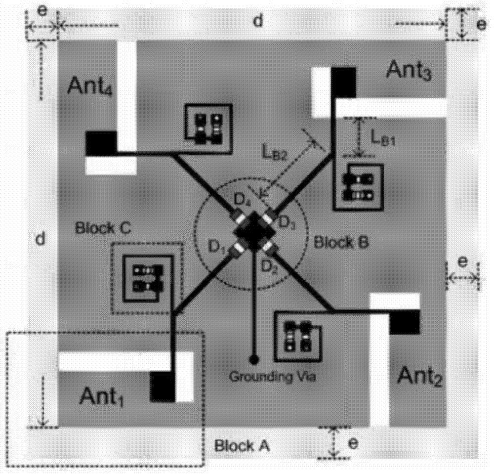
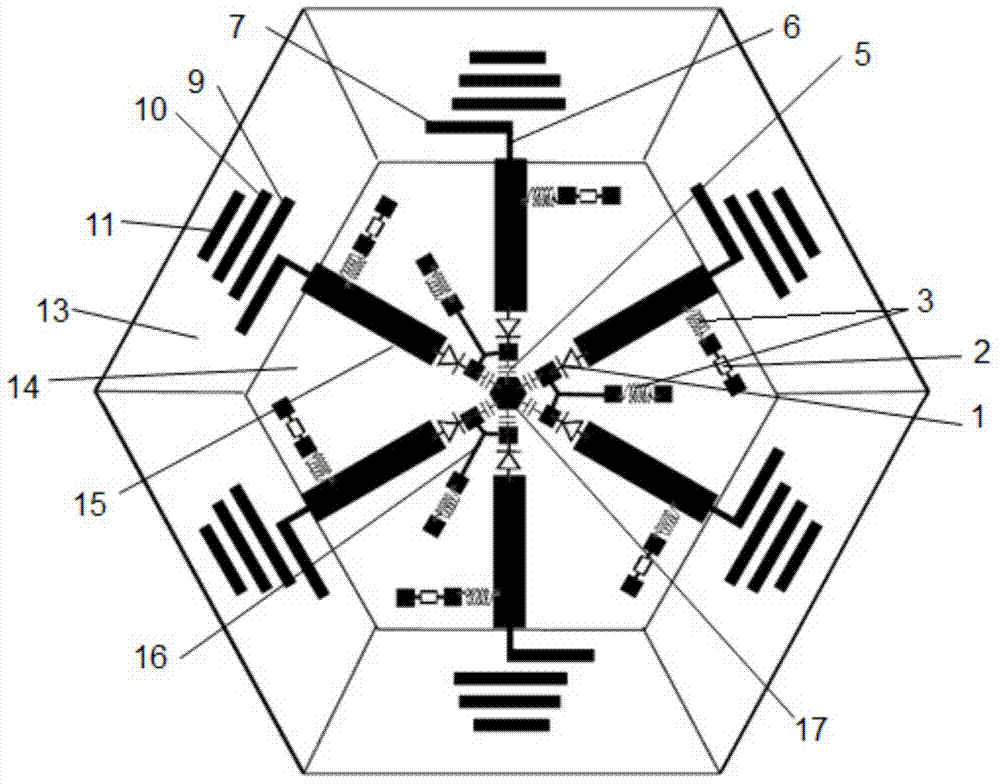
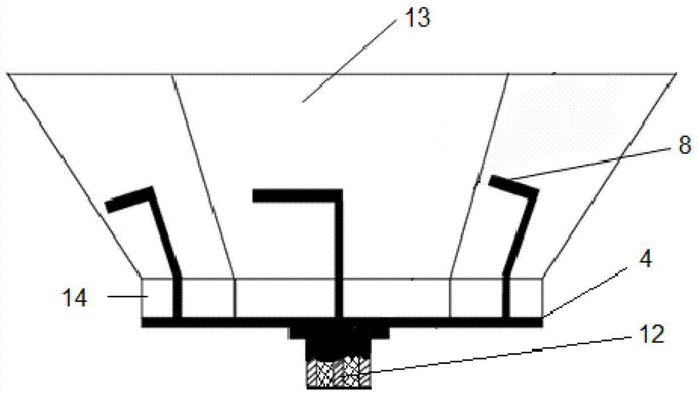
[0017] The trapezoidal insulating dielectric substrate 13 and the regular hexagonal insulating dielectric substrate 14 are polytetrafluoroethylene with a relative permittivity of 2.65 and a thickness of 0.8 mm. The side length of the regular hexagonal insulating dielectric substrate 14 is 32 mm. The upper and lower bottoms of the trapezoidal insulating dielectric substrate 13 32mm and 60mm respectively, the trapezoidal insulating dielectric substrate 13 and the regular hexagonal insulating dielectric substrate 14 form an angle of 120°; the metal floor 4 and the metal patch above the insulating dielectric substrate are copper foils with a thickness of 0.07mm, and the metal floor 4 The side length is 32mm; the characteristic impedance of the coaxial feeder 12 is 50Ω. The side length of the central regular hexagonal metal patch 17 is 3mm, and the size of the first sheet-shaped wire 15 is 4.4*19.5mm 2 ; The size of the second piece of sheet wire 6 is 8*0.7mm 2 ; The size of the h...


PUM

PropertyMeasurementUnit
Angleaaaaaaaaaa

Abstract

The invention discloses an antenna capable of switching wave beam directions. The butterfly-shaped antenna is formed by an orthohexagonal bottom face and six rectangular side faces which are provided with radiators in a printing mode and form certain included angles with the bottom face. Six blocking capacitors are connected on the periphery of a feeding point in an equal angle mode. Each blocking capacitor is respectively and sequentially outward connected with a PIN diode, a metal feeder and a quari-yagi antenna. A high impedance metal wire is educed from a conode of each blocking capacitor and the corresponding PIN diode. Metal wires educed from two adjacent conodes are connected with the same inductor, and the other end of the inductor is connected to a metal pasted floor through a metalized through hole of a medium substrate. An inductor is educed from the side face of each metal feeder, and the other end of the inductor is connected with a voltage reducing resistor. A 5V direct current control signal source controls on-off of the PIN diodes to realize switching of six wave beam states, so that the purposes that antenna radiation covers the whole upper half space, working bandwidth is increased, and radiation to lower half space is shielded are achieved.

Description

technical field [0001] The invention belongs to the field of electronic technology, in particular to an antenna with a switchable beam direction with a PIN diode switch. Background technique [0002] As more and more information content needs to be transmitted, modern communication systems have higher and higher requirements on the information transmission rate in wireless communication, but due to the existence of multipath fading, the data transmission rate decreases with the increase of signal transmission distance . Numerous studies have shown that the proper use of antennas with switchable beams is one way to solve this problem. The switchable beam antenna can change the beam directions of the transmitting and receiving antennas in real time according to changes in the communication environment, thereby effectively reducing noise interference, combating multipath fading, and improving information transmission rates. In vehicle-mounted, airborne or application scenario...

Claims


Application Information

Patent Timeline
IPC IPC(8): H01Q25/04H01Q1/38H01Q23/00
Inventor 王任王秉中丁霄
Owner UNIV OF ELECTRONIC SCI & TECH OF CHINA
Why Eureka
Try Eureka