

Microfluidic devices and their uses
A microfluidic device and microfluidic channel technology, applied in enzymology/microbiology devices, fluid controllers, biochemical cleaning devices, etc., can solve problems such as the need for improvement of microfluidic chips
- Summary
- Abstract
- Description
- Claims
- Application Information
AI Technical Summary
Problems solved by technology
Method used
Image

Examples
Embodiment 1
[0061] Example 1 Genetic identification of fetal nucleated erythrocytes
[0062] 1.15 mL of peripheral blood from the cubital vein of pregnant women at 8-14 weeks of pregnancy, anticoagulated with EDTA-K2, stored with shaking at 4°C, and tested within 24 hours.
[0063] 1.2 Separation of fetal nucleated erythrocytes: Two steps are used for separation. Firstly, separate the red and white blood cells according to the size difference, such as the chip structure in 2.1, remove most red blood cells; pass the recovered cells into the magnetic separation chip, and separate the red and white blood cells by using the magnetic difference of the red and white blood cells.
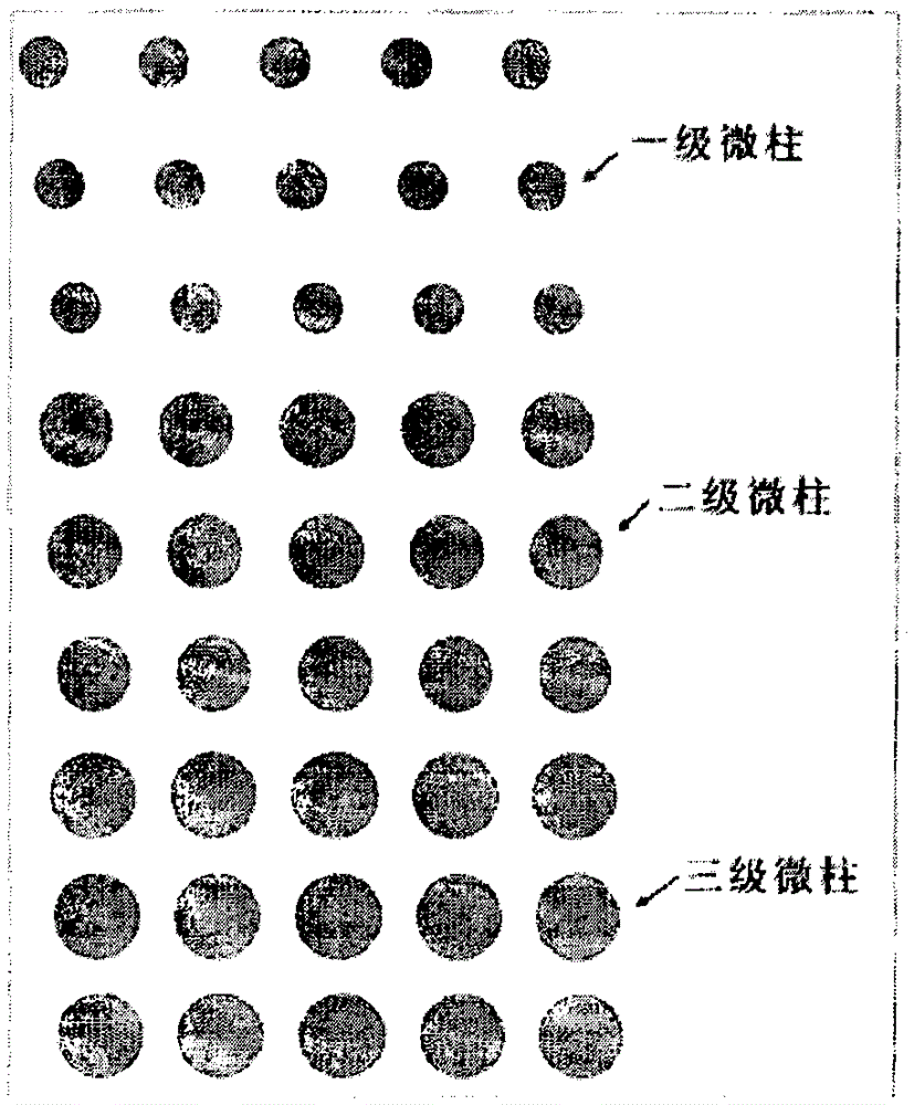
[0064] The structure of the first chip: the spacing between microcolumns is 15 μm, and the relative offset of each row of microcolumns is 6.75 μm. Using deep reactive ion etching technology to build microstructures on silicon wafers, the depth of the channels is 150 μm, and sealing them with glass wafers.
[0065] T...
Embodiment 2
[0071] Example 2: Identification of chromosomal aneuploidy in fetal nucleated erythrocytes
[0072] 2.1 Sampling: Same as 1.1
[0073] 2.2 Separation of fetal nucleated red blood cells:
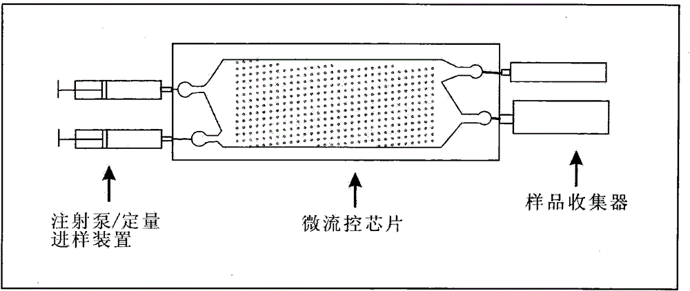
[0074] The structure of the first chip used: as Figure 5 The Nautilus chip in has one sample inlet and 6 sample outlets. The width of the inlet channel is 0.22mm, and the curvature of the channel is gradually enlarged according to a certain ratio. The channel width at the outlet is 3.88mm. The chip channel structure su-8 negative photoresist is used to make a mask by photolithography, and then the PDMS prepolymer is mixed and cast on the mold, and it is formed by turning over the mold. Use glass slides for sealing.
[0075] The structure of the second chip used: as Figure 6 . There are two entrances and two exits. The channel width is 0.5mm and the length is 50mm. The chip channel structure su-8 negative photoresist is used to make a mask by photolithography, and then the PDMS prepol...
Embodiment 3
[0082] Example 3: Screening of circulating tumor cells (CTCs) in cancer patients
[0083] 3.1 Sampling: Take 10 mL of peripheral blood from the cubital vein of tumor patients and anticoagulate with EDTA-K2. Blood samples were stored at 4°C and tested within 24 hours.
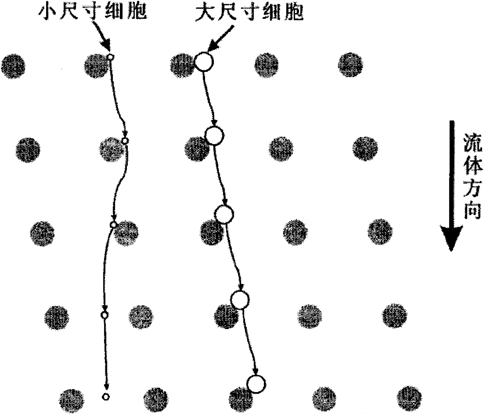
[0084] 3.2 Separation of CTCs: Two-step chip was used for separation. The first step is to separate cells according to their size, such as figure 1 In the chip structure, most of the red blood cells and some extracellular cells were removed; in the second step, EpCAM antibody was used to capture CTCs cells. specifically,
[0085] The structure of the first chip: the spacing between the microcolumns is 20 μm, and the relative offset of each row of microcolumns is 6 μm. Using deep reactive ion etching technology to construct microstructures on silicon wafers, the channel depth is 150mm, and sealing with glass wafers.
[0086] Configuration of the second chip: CTCs were captured using Miltenyi LS / MS Column (M...
PUM
| Property | Measurement | Unit |
|---|---|---|
| width | aaaaa | aaaaa |
| length | aaaaa | aaaaa |
Abstract
Description
Claims
Application Information