LED (light emitting diode) epitaxy structure and application thereof

An epitaxial structure and light-emitting layer technology, applied in electrical components, circuits, semiconductor devices, etc., can solve the problems of reducing luminous efficiency and forward voltage, and achieve high luminous efficiency, reduce negative effects, and improve the effect of lattice quality.

Inactive Publication Date: 2014-03-12
SUZHOU NANOJOIN PHOTONICS
View PDF5 Cites 19 Cited by
  • Summary
  • Abstract
  • Description
  • Claims
  • Application Information

AI Technical Summary

Problems solved by technology

Although the LED epitaxial structure device prepared by this method can effectively reduce the Droop effect, because it introduces a high barrier layer in each quantum well pair, it will lead to a higher forward voltage under high current. reduce light effect

Method used


Image

  • LED (light emitting diode) epitaxy structure and application thereof
  • LED (light emitting diode) epitaxy structure and application thereof
  • LED (light emitting diode) epitaxy structure and application thereof

Examples


Embodiment 1

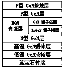
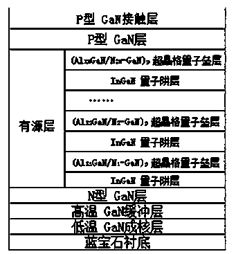
[0026] Conventional LED epitaxial structures such as figure 1 As shown, the structure of this embodiment is as figure 2 As shown, specifically, the GaN nucleation layer, the GaN buffer layer, the n-type GaN layer, the MQW light-emitting layer with 15 pairs of repeated periods, and the p-type GaN layer and p-type contact layer are grown sequentially on the sapphire substrate by MOCVD method. . The number of pairs of AlGaN / n-GaN superlattice quantum barrier layers in each pair of MQW light-emitting layers is 5 pairs, 5 pairs of superlattice quantum barrier layers have the same Al composition content and the same n-type doping concentration value, and 15 pairs The total thickness of the MQW light-emitting layer with superlattice quantum barriers is 225nm, of which the total thickness of quantum well layers is 45nm, the total thickness of superlattice quantum barrier layers is 180nm, and the total thickness of each pair of AlGaN / n-GaN superlattice quantum barrier layers is 12nm...

Embodiment 2

[0031]Different from the optimization scheme of the exponential gradient mode for the Al component and n-type impurity concentration proportional coefficient in Example 1, this embodiment adopts the stepwise linear increase and then linear decrease of the Al component and n-type impurity concentration proportional coefficient.

[0032] Each MQW light-emitting layer group is composed of several pairs of MQW light-emitting layer pairs with the same characteristics of AlGaN / n-GaN superlattice quantum barrier layers, and Al(m) represents the AlGaN / n-GaN superlattice in the mth group of MQW light-emitting layer The Al composition value in the quantum barrier layer pair, N(m) represents the n-type impurity concentration value in the AlGaN / n-GaN superlattice quantum barrier layer pair in the m-th group of MQW light-emitting layers, from the first pair of MQW light-emitting layers to the first For the MQW light-emitting layer, the change trend of the Al (m) is linearly increasing, and...


PUM


Abstract

The invention provides an LED (light emitting diode) epitaxy structure. The LED epitaxy structure sequentially comprises a substrate, a GaN nucleating layer, a GaN buffer layer, an n-type GaN layer, an active layer, a p-type GaN layer and a p-type contact layer from top to bottom; the active layer is provided with at least two pairs of MQW (multiple quantum well) luminous layers; each MQW luminous layer comprises a superlattice quantum base layer and a quantum well layer; each superlattice quantum base layer is formed by alternately stacking AlGaN/n-GaN; each quantum well layer consists of InGaN; AlGaN/n-GaN superlattice quantum base layer centering Al component values trend to linearly rise stably and then linearly fall stably; and n-type impurity concentration values trend to linearly rise stably and then linearly fall stably. The LED epitaxy structure has the advantages that the MQW lattice quality can be effectively improved; the capture probability on electrons or cavities of each quantum well in the active layer is greatly improved, a Droop negative effect on devices is effectively redcued, the internal quantum efficiency of the LED devices is improved, the LED epitaxy structure can be well applied to a high-power device, and the high photosynthetic efficiency of the device is kept.

Description

technical field [0001] The invention relates to an LED epitaxial structure that can be applied to high-power devices and can maintain high light efficiency values ​​of the devices. Background technique [0002] At present, commercial LED epitaxial wafers are mostly made by MOCVD. Because GaN material has a series of advantages such as wide band gap, high electron mobility, high thermal conductivity, high hardness, high stable chemical properties, small dielectric constant and high temperature resistance, it is widely used in commercial high-brightness light-emitting diodes and semiconductors. Laser has a wide range of practical application value and huge market potential. The existing GaN-based LED epitaxial structures widely used in actual production generally include: low-temperature GaN buffer layer, high-temperature GaN buffer layer, n-type doped GaN layer, MQW active layer, p-type AlGaN electron blocking layer, p-type Doped GaN layer, p-type GaN contact layer. Among ...

Claims


Application Information

Patent Timeline
Patent Type & Authority Applications(China)
IPC IPC(8): H01L33/06
CPCH01L33/06H01L33/32
Inventor 南琦
Owner SUZHOU NANOJOIN PHOTONICS
Why Eureka
Try Eureka