Crystal silicon surface femtosecond laser selective ablation method based on electron dynamic control

An electronic dynamic control, femtosecond laser technology, applied in the field of femtosecond laser applications, can solve the problem of not considering material properties, and achieve the effect of improving processing accuracy and processing efficiency

Active Publication Date: 2014-03-26
BEIJING INSTITUTE OF TECHNOLOGYGY
View PDF6 Cites 31 Cited by
  • Summary
  • Abstract
  • Description
  • Claims
  • Application Information

AI Technical Summary

Problems solved by technology

However, the research on the generation of periodic corrugated micro-nano structures on the surface of materials induced by femtosecond lasers mainly focuses on the property of the laser itself—the polarization state, without considering the properties of the material itself.

Method used


Image

  • Crystal silicon surface femtosecond laser selective ablation method based on electron dynamic control
  • Crystal silicon surface femtosecond laser selective ablation method based on electron dynamic control

Examples


Embodiment Construction

[0023] The present invention will be further introduced below in conjunction with the accompanying drawings and embodiments.

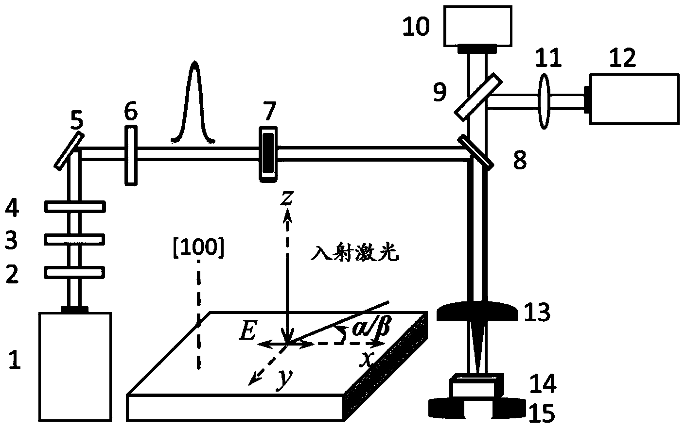
[0024] In this embodiment, the processing method of controlling the femtosecond laser-induced selective ablation of periodic corrugated micro-nano structures on the surface of crystal silicon, the specific processing optical path is as follows figure 1 shown. The processing optical path is that the femtosecond laser 1 generates femtosecond laser pulses. After the femtosecond laser pulses pass through the first half-wave plate 2, the polarizer 3, and the second half-wave plate 4, they are reflected by the first mirror 5 and pass through a quarter A wave plate 6 and a mechanical switch 7 are reflected by the second reflector 8 and focus on the surface of the sample 14 after being reflected by the achromatic double-glued plano-convex lens 13. The sample 14 to be processed is fixed on the six-dimensional mobile platform 15; the white light source 10 passes...


PUM


Abstract

The invention relates to a crystal silicon surface femtosecond laser selective ablation method based on electron dynamic control, and belongs to the technical field of femtosecond laser application. The crystal silicon surface femtosecond laser selective ablation method based on the electron dynamic control enables laser polarization parameters and crystal lattice properties of crystal silicon materials to be integrated, through the operation that femtosecond laser rays or the included angel of elliptic polarization and monocrystal silicon is adjusted effectively, the selective induction generation of crystal silicon surface periodical ripple micro nano structures is controlled by regulating and controlling material surface instant electron excitation dynamic states, and the induction generation of the crystal silicon surface periodical ripple micro nano structures can be achieved effectively and accurately according to preliminary design. According to the crystal silicon face femtosecond laser selective ablation method based on the electron dynamic control, selective ablation control is carried out on the silicon surface periodic ripple nano structures with diamond lattice structures from the aspect of static laser irradiation and the aspect of laser direct writing, the processing accuracy and the processing efficiency of the surface processing of the silicon surface periodic ripple nano structures are improved greatly, and the application value of the method on the aspects such as information storage is high.

Description

technical field [0001] The invention relates to a femtosecond laser selective ablation method on the surface of crystal silicon based on electronic dynamic control, and belongs to the technical field of femtosecond laser application. Background technique [0002] The micro-nano structure on the surface of single crystal silicon is a focus in the field of semiconductor and crystalline silicon solar energy research, because the micro-nano structure on the surface of single crystal silicon is closely related to the photoelectric performance of the crystal. Therefore, it has become a research focus to effectively adjust the micro-nano structure of silicon surface. With the emergence of mode-locking and amplification technology, femtosecond laser technology has developed rapidly. Compared with traditional long-pulse laser processing, femtosecond laser processing has incomparable advantages, mainly in extremely high peak power and small damage threshold, small processing heat-aff...

Claims


Application Information

Patent Timeline
Patent Type & Authority Applications(China)
IPC IPC(8): B23K26/362B23K26/064
CPCB23K26/0622B23K26/0643B23K26/0648B23K26/361B23K26/40B23K2103/50
Inventor 姜澜韩伟娜李晓炜
Owner BEIJING INSTITUTE OF TECHNOLOGYGY
Why Eureka
Try Eureka