Semi-conductor device with self-aligning contact holes and manufacture method of semi-conductor device

A self-aligned contact hole, semiconductor technology, applied in the direction of semiconductor devices, semiconductor/solid-state device manufacturing, semiconductor/solid-state device components, etc., can solve problems such as no effective means proposed

Active Publication Date: 2014-03-26
SEMICON MFG INT (SHANGHAI) CORP
View PDF5 Cites 11 Cited by
  • Summary
  • Abstract
  • Description
  • Claims
  • Application Information

AI Technical Summary

Problems solved by technology

[0010] How to combine the "gate-last process" and "self-aligned contact hole preparation process" to produc

Method used


Image

  • Semi-conductor device with self-aligning contact holes and manufacture method of semi-conductor device
  • Semi-conductor device with self-aligning contact holes and manufacture method of semi-conductor device
  • Semi-conductor device with self-aligning contact holes and manufacture method of semi-conductor device

Examples


preparation example Construction

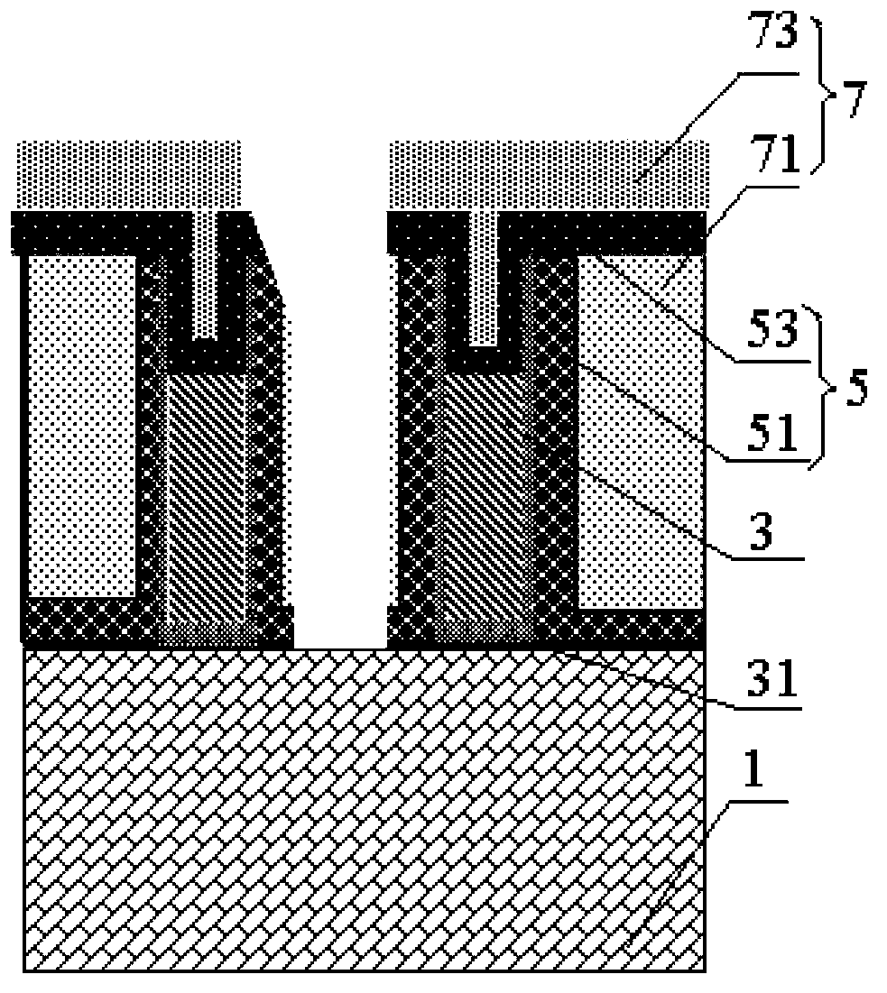
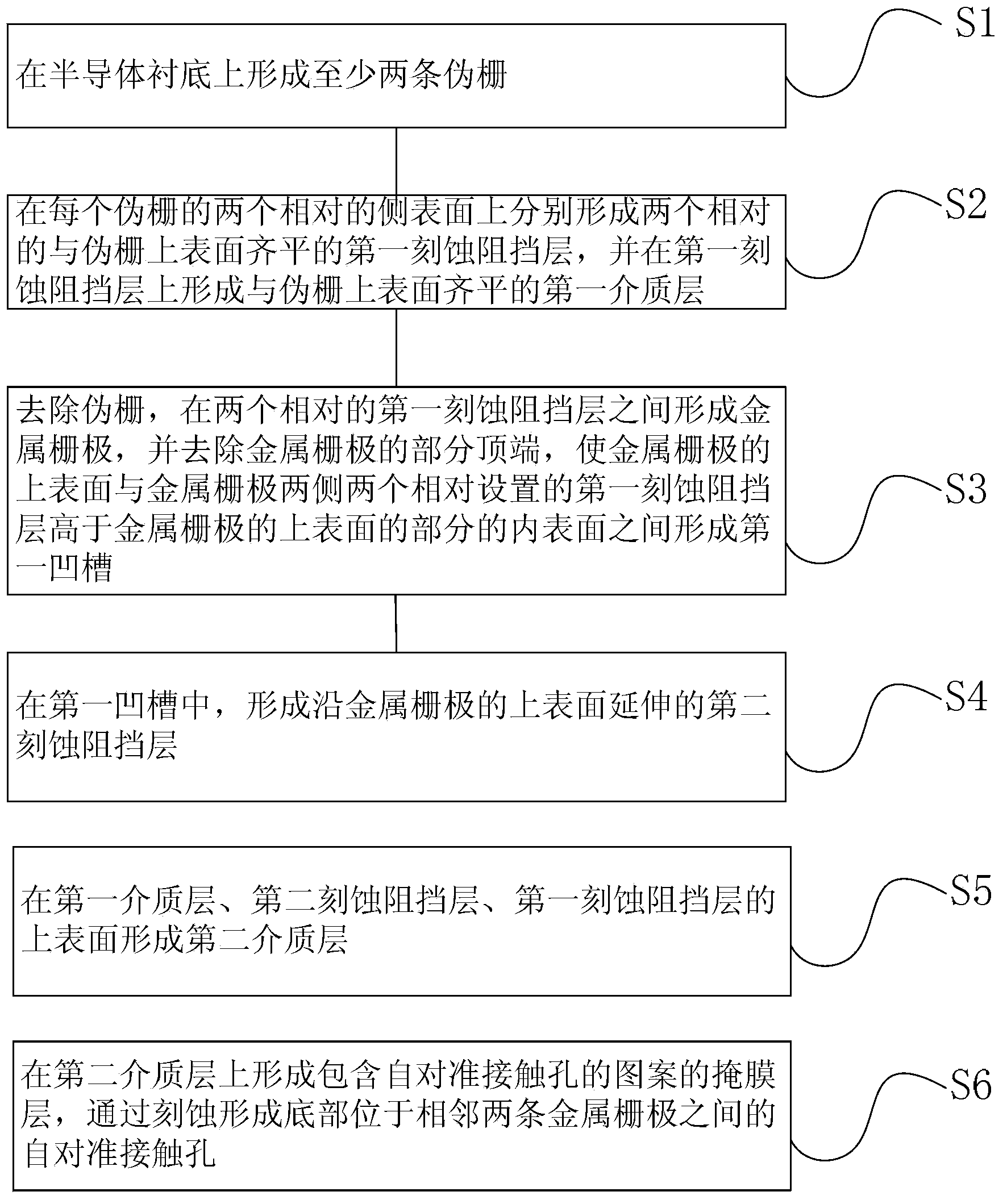
[0061] At the same time, in an embodiment of the present application, a method for preparing a semiconductor device with self-aligned contact holes is also provided, such as figure 2 As shown in the flow chart, the method includes the following steps: S1, forming at least two dummy gates 3' on the semiconductor substrate 1. S2. On the two opposite side surfaces of each dummy gate 3′, respectively form two opposite first etch barrier layers 51 flush with the upper surface of the dummy gate 3′, and form on the first etch barrier layer 51 A first dielectric layer 71 flush with the upper surface of the dummy gate 3′. S3, remove the dummy gate 3', form the metal gate 3 between the two opposite first etching barrier layers 51, and remove part of the top of the metal gate 3, so that the upper surface of the metal gate 3 is aligned with the metal gate 3 A first groove is formed between the inner surfaces of the portions of the first etch barrier layer 51 disposed opposite to each ot...

Embodiment 1

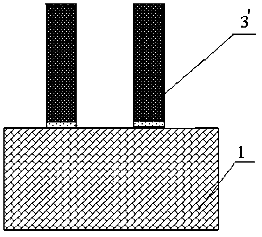
[0075] The following will combine Figure 3a to Figure 3d The specific operation steps of an embodiment of the method for manufacturing a semiconductor device with self-aligned contact holes according to the present application will be described in detail. Figure 3a to Figure 3d A schematic cross-sectional structure diagram of a substrate in each step in the first embodiment of the method for manufacturing a semiconductor device according to the present application is shown.

[0076] S1, such as Figure 3a As shown, at least two dummy gates 3' are formed on the semiconductor substrate 1. Wherein, the substrate 1 may be a single crystal silicon or a polycrystalline silicon substrate, and may also be a silicon-on-insulator, and a source electrode and a drain electrode (not shown in the figure) are formed in the substrate 1 . The formed dummy gate 3' is a gate made of polysilicon material. In actual operation, before forming the dummy gate 3', a dummy gate dielectric layer ma...

Embodiment 2

[0089] A method for preparing a semiconductor device with self-aligned contact holes comprises the following steps:

[0090] Steps S1 to S3 are the same as in Embodiment 1.

[0091] Step S4, using the SiN material with a high selective etching ratio of 8 to the first dielectric layer 71, to form a second etch that extends continuously on the upper surfaces of the metal gate 3, the first etch stop layer 51, and the first dielectric layer 71. etch stop layer 53. The second etch barrier layer 53 is formed by chemical vapor deposition.

[0092] Step S5 , forming a second dielectric layer 73 on the upper surface of the second etch stop layer 53 . The material of the formed second dielectric layer 73 is an insulating material with a low dielectric constant. The second dielectric layer 73 is formed by chemical vapor deposition. After the second dielectric layer 73 is deposited, chemical mechanical polishing can be used to planarize the surface.

[0093] Step S6, the step of form...


PUM


Abstract

The invention provides a semi-conductor device with self-aligning contact holes and a manufacture method of the semi-conductor device. The semi-conductor device comprises a semiconductor substrate, at least two metal grids, etched barrier layers and dielectric layers, wherein the etched barrier layers are formed on the surfaces of the metal grids; each etched barrier layer comprises a first etched barrier layer and a second etched barrier layer; the dielectric layers are formed on the etched barrier layers; each dielectric layer comprises a first dielectric layer and a second dielectric layer. As the upper surfaces of the metal grids are lower than those of the first etched barrier layers, the metal grids and the first etch barrier layers are different in height; the second etched barrier layers are arranged in first grooves formed between the upper surfaces of the metal grids and the upper surfaces, relative to the metal grids, of the first etched barrier layers, so as to improve the anti-etch capability of the upper parts of the metal grids. The phenomenon of the short circuit communication between the self-aligning contact holes and the metal grids caused when the metal grids are exposed during the forming of the self-aligning contact holes is eliminated.

Description

technical field [0001] The invention belongs to the field of semiconductors, in particular to a semiconductor device with a self-aligned contact hole and a preparation method thereof. Background technique [0002] With the decreasing size of semiconductor devices, more and more device units are integrated per unit area, the density of devices is gradually increasing, and the size of devices is continuously decreasing, which also increases the difficulty of manufacturing. In the face of the problems in the manufacture of semiconductor devices, researchers have made a lot of improvements, such as: [0003] At present, the commonly used gate forming process is the front-gate process. The so-called front-gate process refers to first depositing a gate dielectric layer, forming a gate on the gate dielectric layer, and then performing source and drain implantation, and then performing an annealing process to activate the source. The ions in the drain form the source and drain regi...

Claims


Application Information

Patent Timeline
IPC IPC(8): H01L23/528H01L21/768
CPCH01L27/088H01L29/66477H01L21/82345H01L29/4966H01L29/66545
Inventor 洪中山
Owner SEMICON MFG INT (SHANGHAI) CORP
Why Eureka
Try Eureka