
Transversal bipolar transistor with low-ratio on-resistance

A technology of bipolar transistors and specific on-resistance, which is applied in the direction of semiconductor devices, circuits, electrical components, etc., can solve the problems of low specific on-resistance and the inability to increase the reverse conduction voltage and specific on-resistance, and achieve a reduction The effect of specific on-resistance, high reverse blocking voltage, and improved withstand voltage level

Inactive Publication Date: 2014-03-26
SUZHOU YINGNENG ELECTRONICS TECH
View PDF4 Cites 1 Cited by
  • Summary
  • Abstract
  • Description
  • Claims
  • Application Information

AI Technical Summary

Problems solved by technology

[0005] For this reason, what the present invention is to solve is that the dopant dose in the drift region of the lateral bipolar transistor with the existing SINGLE RESURF structure has an opposite effect on the reverse blocking voltage and the specific on-resistance, which can not give consideration to improving the reverse conduction. Voltage and at the same time reduce the technical problem of specific on-resistance, and provide a lateral bipolar transistor with low specific on-resistance

Method used


Image

  • Transversal bipolar transistor with low-ratio on-resistance
  • Transversal bipolar transistor with low-ratio on-resistance

Examples


Embodiment Construction

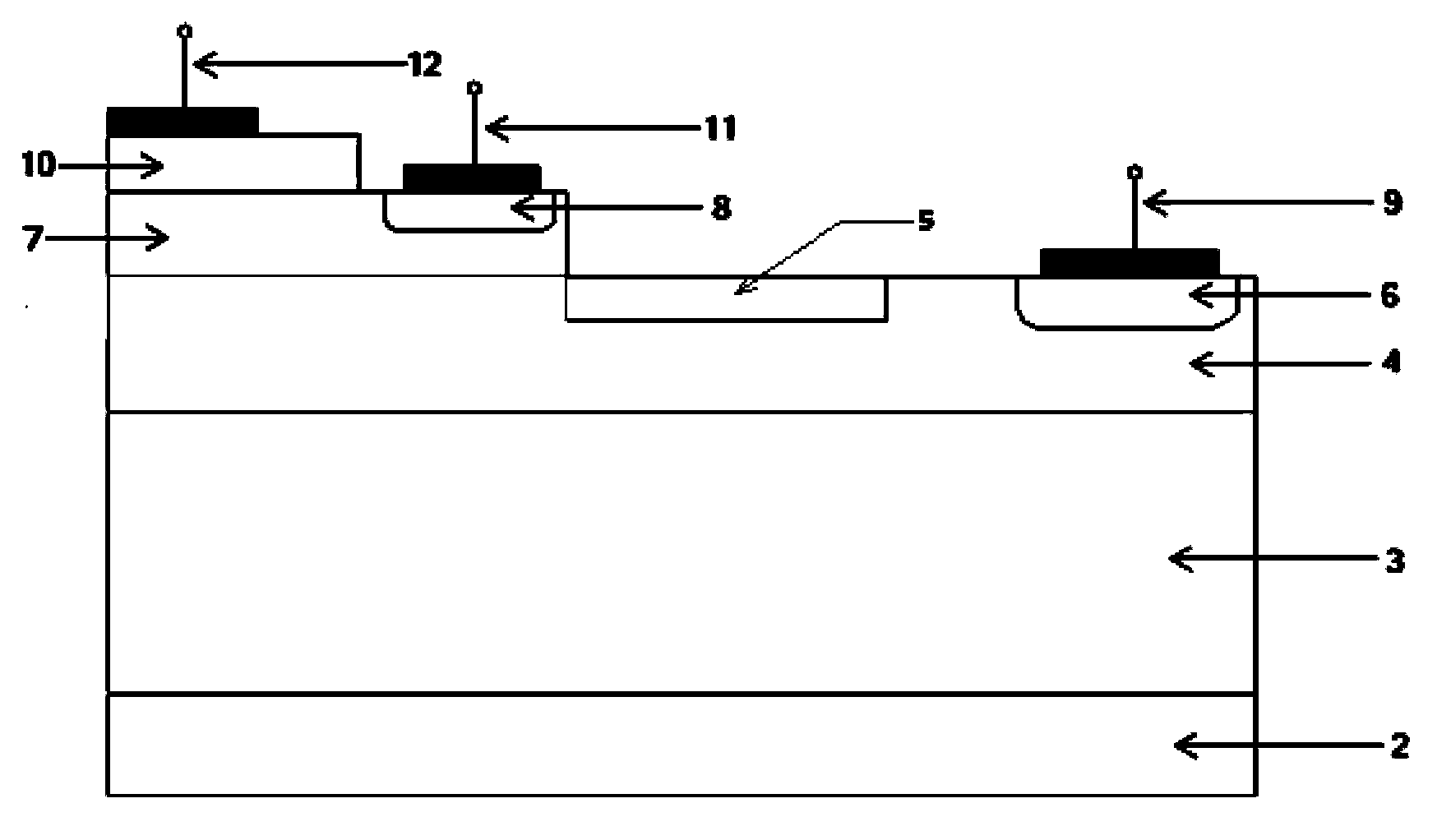
[0033] See figure 1 As shown, the NPN type lateral bipolar transistor of the first embodiment of the present invention includes from bottom to top:

[0034] P+ silicon carbide substrate 2;

[0035] P-silicon carbide epitaxial layer, the P-silicon carbide epitaxial layer constitutes the P-type first RESURF region 3;

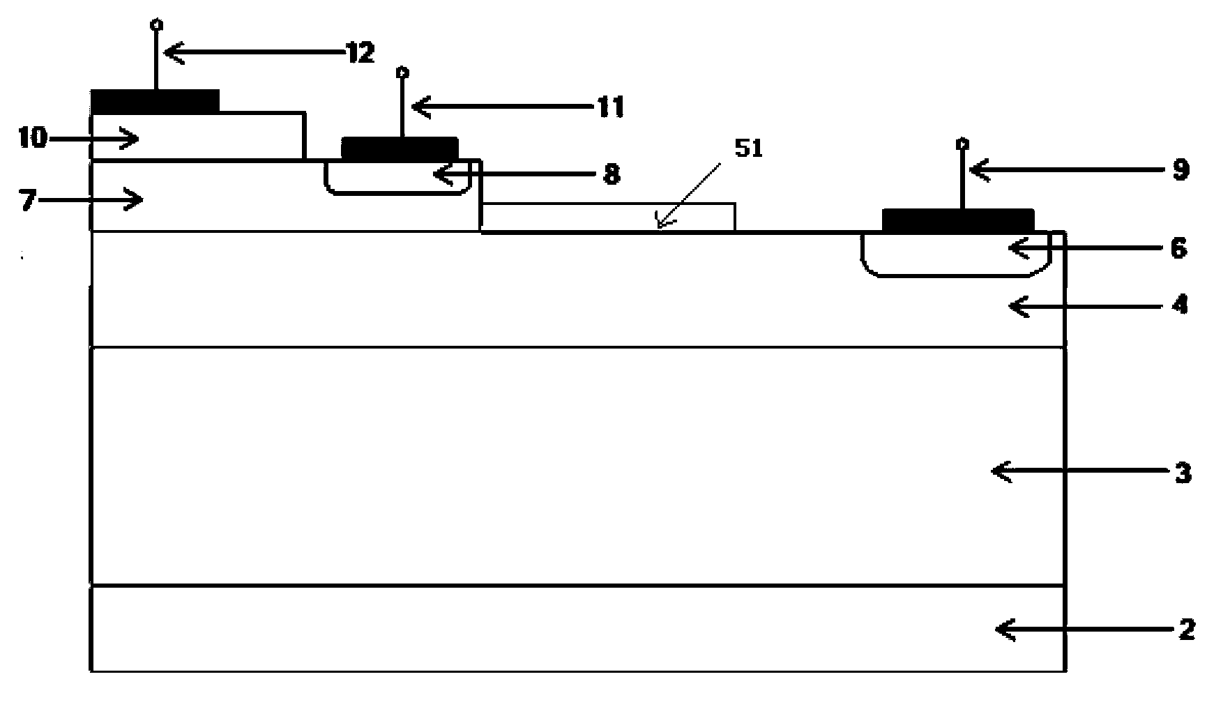
[0036] An N-type collector region 4 is formed by epitaxy on the P-silicon carbide, and N-type collector region 4 is formed near the upper surface by ion implantation. + Collector area ohmic contact area 6 and injection type second RESURF area 5, wherein a collector 9 is provided on said N+ collector area ohmic contact area 6; said injection type second RESURF area 5 is used to smooth the electric field of the drift area As a variation, as a specific embodiment of the present invention, the second RESURF region 5 is a P-type RESURF region, and the length of the second RESURF region 5 is two-thirds of the length of the drift region of the lateral bipolar transistor, The t...


PUM


Abstract

The invention discloses a transversal bipolar transistor with low-ratio on-resistance. The transversal bipolar transistor comprises a substrate, a first RESURF region on the substrate, a collector region, a base region, and an emitter region, and further comprises a second RESURF region for smoothing the electric field change of a drift region, wherein the collector region, the base region and the emitter region are arranged in sequence; a base region ohmic contact region is formed in the base region; a base electrode is arranged on the base region ohmic contact region; a collector region ohmic contact region is formed in the collector region; a collector electrode is arranged on the collector region ohmic contact region; an emitting electrode is arranged on the emitter region. Through the arrangement of the second RESURF region, the electric field of the drift region of the transversal bipolar transistor can be smooth, so that the reverse blocking voltage can be higher and the on-resistance can be lower under the condition that the drift region length is not changed.

Description

Technical field [0001] The invention relates to a power semiconductor device and a manufacturing method thereof, in particular to a lateral bipolar transistor with low specific on-resistance. Background technique [0002] Power semiconductor devices are also called electronic power devices. With the development of power integrated circuits, especially monolithic power integrated systems, power semiconductor devices are booming. The electrodes of the lateral power devices are located on the surface of the chip, and it is easy to achieve mutual integration with low-voltage signal circuits and other devices through internal connections. Therefore, the lateral power devices are widely used in power integrated circuits. In power integrated circuits, lateral power devices often account for more than half of the entire chip area, which is the core and key of the entire power integrated circuit. Moreover, with the development of modern power integrated circuits, higher requirements have...

Claims


Application Information

Patent Timeline
Patent Type & Authority Applications(China)
IPC IPC(8): H01L29/739H01L29/06
CPCH01L29/735H01L29/063
Inventor 张作钦崔京京
Owner SUZHOU YINGNENG ELECTRONICS TECH
Learn More