Preparation method of flexible substrate silicon nanowire heterojunction solar cell

A technology of silicon nanowires and flexible substrates, applied in the field of solar cells, can solve problems such as impossible industrial production

Inactive Publication Date: 2014-03-26
CHANGZHOU UNIV
View PDF6 Cites 10 Cited by
  • Summary
  • Abstract
  • Description
  • Claims
  • Application Information

AI Technical Summary

Problems solved by technology

[0002]Si nanowire structure has become a powerful photovoltaic material due to its optical properties of anti-reflection and strong absorption and electrical properties of high carrier mobility. Candidate; researchers at Harvard University obtained a single p-i-n radial silicon nanowire battery, and its conversion efficiency reached 3.4% [Tian B Z et a1. Coaxial silicon nanowires as solar cells and nanoelectronie power sources. nature, 2007, 449(7164): 885-890]; the introduction of the radial structure mak

Method used


Image

  • Preparation method of flexible substrate silicon nanowire heterojunction solar cell
  • Preparation method of flexible substrate silicon nanowire heterojunction solar cell

Examples


example 1

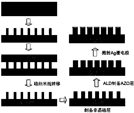
[0026] Example one Copper foil / p-type monocrystalline silicon nanowire / amorphous silicon passivation layer / n-type silicon thin film / AZO / Ag solar cell

[0027] 1. Preparation of single crystal silicon nanowires with a length of 6 μm:

[0028] A (100) doped p-type silicon wafer is selected, with a resistivity of 1.5 Ωcm and a thickness of 180 μm.

[0029] Dip the silicon wafer into acetone and ethanol for 10 min and ultrasonically clean it to remove the organic impurities on the surface, wash it with deionized water; then immerse it in concentrated H 2 SO 4 :H 2 o 2 =3:1 (volume ratio) mixed solution was boiled at 130°C for 10 min, rinsed with deionized water, and dried with nitrogen gas for later use.

[0030] The easy-to-transfer silicon nanowire arrays were prepared by secondary etching. First, the silicon wafer was immersed in 0.005M AgNO 3 and 5M HF mixed solution for 1min, that is, spread a layer of silver on the surface of the silicon wafer, rinse with deionized wa...

example 2

[0042] Example two Copper foil / n-type monocrystalline silicon nanowire / amorphous silicon passivation layer / p-type silicon film / AZO layer / Ag solar cell

[0043] 1. Preparation of single crystal silicon nanowires with a length of 8 μm:

[0044] A (100) doped n-type silicon wafer is selected, with a resistivity of 1.5 Ωcm and a thickness of 180 μm.

[0045] The steps are the same as step 1 in Example 1, but the corrosion time is 1.3h, as follows:

[0046] Dip the silicon wafer into acetone and ethanol for 10 min and ultrasonically clean it to remove the organic impurities on the surface, wash it with deionized water; then immerse it in concentrated H 2 SO 4 :H 2 o 2 =3:1 (volume ratio) mixed solution was boiled at 130°C for 10 min, rinsed with deionized water, and dried with nitrogen gas for later use.

[0047] The easy-to-transfer silicon nanowire arrays were prepared by secondary etching. First, the silicon wafer was immersed in 0.005M AgNO 3 and 5M HF mixed solution fo...


PUM

PropertyMeasurementUnit
Resistivityaaaaaaaaaa
Thicknessaaaaaaaaaa
Thicknessaaaaaaaaaa

Abstract

The invention relates to solar cells, in particular to a preparation method of a flexible substrate silicon nanowire heterojunction solar cell. Excellent light absorbing characteristics of silicon nanowires are brought into full play. The preparation method includes utilizing a wet etching process to prepare a monocrystalline silicon nanowire array on a monocrystalline silicon substrate, adopting a copper electroconductive adhesive tape to transfer silicon nanowires on copper foil, and preparing a silicon nanowire cell. Being different from a method that a silicon nanowire array on a monocrystalline silicon substrate is directly utilized to prepare a cell, the preparation method sequentially includes the steps of transferring the silicon nanowires on a flexible substrate and preparing the silicon nanowire cell, so that the monocrystalline silicon substrate can be repeatedly used, silicon consumption is reduced, and material cost is saved.

Description

technical field [0001] The invention relates to a solar cell, in particular to transferring a silicon nanowire array to a metal foil to prepare a nanowire heterojunction solar cell. Background technique [0002] Due to its optical properties of antireflection and strong absorption and electrical properties of high carrier mobility, silicon nanowire structure has become a strong candidate for photovoltaic materials; researchers at Harvard University have obtained a single p-i-n radial Silicon nanowire cells, the conversion efficiency reached 3.4% [Tian B Z et a1. Coaxial silicon nanowires as solar cells and nanoelectronie power sources. nature, 2007, 449(7164): 885-890]; the introduction of the radial structure makes the light absorption and photogenerated carrier transport direction orthogonal, thus solving the contradiction between light absorption and photogenerated carrier separation, but This method utilizes the micromachining technology of a single nanowire operation,...

Claims


Application Information

Patent Timeline
IPC IPC(8): H01L31/18H01L31/20
CPCB82Y30/00B82Y40/00H01L31/202Y02E10/50Y02P70/50
Inventor 丁建宁李坤堂袁宁一陆鹏飞房香柏丽
Owner CHANGZHOU UNIV
Why Eureka
Try Eureka