
Multilayer structure composite transparent conducting thin film based on silver nanowires and preparation method thereof

A technology of transparent conductive film and multi-layer structure, which is applied to conductive layers on insulating carriers, cable/conductor manufacturing, circuits, etc., can solve the problems of poor conductivity and low conductivity of the final film, so as to reduce production costs and prevent oxidation. , the effect of improving adhesion

Active Publication Date: 2014-04-16
CHANGZHOU HUAWEI ADVANCED MATERIAL
View PDF7 Cites 19 Cited by
  • Summary
  • Abstract
  • Description
  • Claims
  • Application Information

AI Technical Summary

Problems solved by technology

However, the electrical conductivity of general organic polymers is poor, and the electrical conductivity of the final film formed is not high.

Method used


Image

  • Multilayer structure composite transparent conducting thin film based on silver nanowires and preparation method thereof
  • Multilayer structure composite transparent conducting thin film based on silver nanowires and preparation method thereof
  • Multilayer structure composite transparent conducting thin film based on silver nanowires and preparation method thereof

Examples


Embodiment 1

[0053] The preparation method of the composite transparent conductive film of the silver nanowire-based multilayer structure of the present embodiment comprises the following steps:

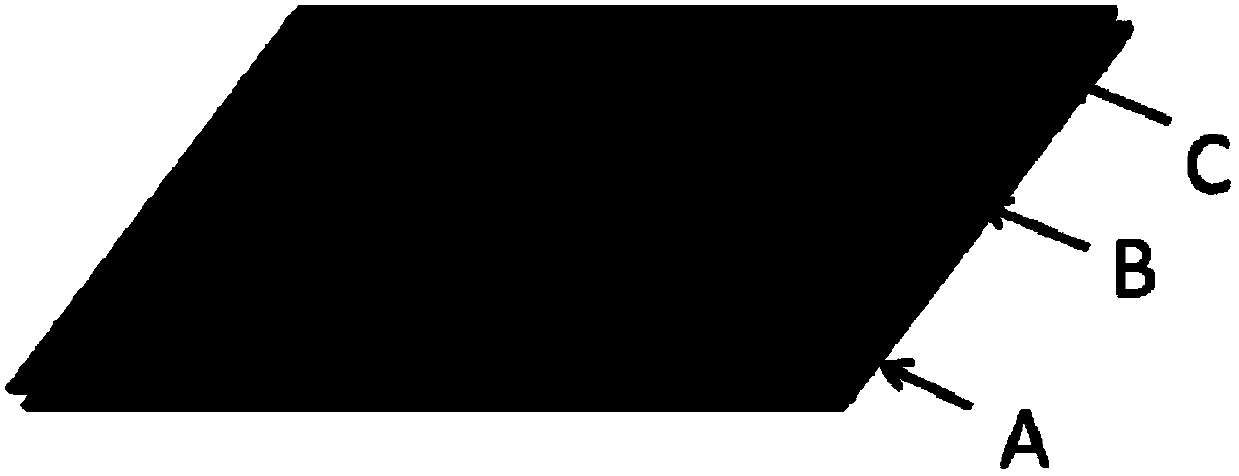
[0054] (1) At 25°C, a layer of AZO film with a thickness of 50nm is prepared on the PET substrate by magnetron sputtering, that is, the lower AZO conductive layer A. The sputtering conditions are: the sputtering gas is high-purity argon, and the sputtering gas is The pressure is 0.4Pa, and the aluminum oxide doped zinc oxide ceramic target is used in this embodiment, and the mass percentage of aluminum oxide is 2%;

[0055] (2) Prepare a silver nanowire suspension, and apply the silver nanowire suspension to the lower AZO conductive layer A by spin coating to form a silver nanowire conductive layer B, wherein the silver nanowire suspension is prepared Include the following steps:

[0056] (2-1) Magnetically stir 50ml of 0.15mol / L polyvinylpyrrolidone solution in ethylene glycol under heating at ...

Embodiment 2

[0068] The preparation method of the composite transparent conductive film of the silver nanowire-based multilayer structure of the present embodiment comprises the following steps:

[0069] (1) At 25°C, a layer of AZO film with a thickness of 300nm is prepared on the PET substrate by magnetron sputtering, that is, the lower AZO conductive layer A. The sputtering conditions are: the sputtering gas is high-purity argon, and the sputtering gas is The pressure is 0.5Pa, and the aluminum oxide doped zinc oxide ceramic target is used in this embodiment, and the mass percentage of aluminum oxide is 2%;

[0070] (2) Prepare a silver nanowire suspension, and apply the silver nanowire suspension to the lower AZO conductive layer A by spin coating to form a silver nanowire conductive layer B, wherein the silver nanowire suspension is prepared Include the following steps:

[0071] (2-1) Heat 50ml of 0.3mol / L polyvinylpyrrolidone in ethylene glycol under magnetic stirring at 180°C, and c...

Embodiment 3

[0079] The preparation method of the composite transparent conductive film of the silver nanowire-based multilayer structure of the present embodiment comprises the following steps:

[0080] (1) At a temperature of 150°C, a layer of AZO film with a thickness of 100nm was prepared on a PI substrate by magnetron sputtering to form a lower AZO conductive layer A. The sputtering conditions were: the sputtering gas was high-purity argon, The sputtering pressure is 0.6Pa, and the aluminum oxide-doped zinc oxide ceramic target is used in this embodiment, and the mass percentage of aluminum oxide is 1%;

[0081] (2) Prepare a silver nanowire suspension, and apply the silver nanowire suspension to the lower AZO conductive layer A by spin coating to form a silver nanowire conductive layer B, wherein the silver nanowire suspension is prepared Include the following steps:

[0082] (2-1) Magnetically stir 50ml of 0.3mol / L polyvinylpyrrolidone solution in ethylene glycol under heating at 1...


PUM

PropertyMeasurementUnit
particle diameteraaaaaaaaaa
lengthaaaaaaaaaa
thicknessaaaaaaaaaa

Abstract

The invention discloses a multilayer structure composite transparent conducting thin film based on silver nanowires and a preparation method thereof. A lower AZO conducting layer, a silver nanowire conducting layer, an upper AZO conducting layer and another silver nanowire conducting layer are sequentially prepared on a flexible substrate, wherein in the process that a polyol process is adopted to prepare the silver nanowire conducting layers, the molar ratio of polyvinylpyrrolidone to metal salt to hydrogen nitrate to silver nitrate is 1.5-6 to 1.5*10-3-3*10-3 to 0.01-0.5 to 1. Adhesivity and stability of the multilayer structure composite transparent conducting thin film based on the silver nanowires are improved, improvement of stability and electrical conductivity of the composite transparent conducting thin film based on the silver nanowires is facilitated, the AZO thin film and the flexible substrate are adopted, preparation cost is reduced, and flexibility of materials is increased. The composite transparent conducting thin film based on the silver nanowires is applied to flexible electronic devices, device integration is easy to achieve, the preparation technology is simple, and the composite transparent conducting thin film based on the silver nanowires is suitable for industrial production.

Description

technical field [0001] The invention relates to the field of semiconductors, in particular to a composite transparent conductive film with a silver nanowire-based multilayer structure and a preparation method thereof. Background technique [0002] As a special material that is both transparent and conductive, transparent conductive films are widely used in liquid crystal displays (LCDs), touch screens (Touch screens), light-emitting diodes (LEDs), solar cells (Solar cells) and other fields. Indium tin oxide (ITO) has high transmittance and low resistivity, making it the most widely used transparent conductive film. However, since indium is a precious metal, its price is relatively high, which makes the final ITO film cost relatively high, and indium is poisonous and easy to pollute the environment. Therefore, aluminum-doped zinc oxide film (AZO), as a lower-cost transparent conductive film, has become one of the main substitutes for ITO at present. However, AZO or ITO film...

Claims


Application Information

Patent Timeline
Patent Type & Authority Applications(China)
IPC IPC(8): H01B5/14H01B13/00
Inventor 沈文锋徐青松黄琦金杨晔宋伟杰
Owner CHANGZHOU HUAWEI ADVANCED MATERIAL
Learn More