Electric conducting plug and forming method of electric conducting plug

A technology of conductive plugs and conductive materials, applied in circuits, electrical components, electrical solid devices, etc., can solve problems such as performance degradation of semiconductor devices, and achieve the effect of good performance and avoidance of corrosion

Active Publication Date: 2014-04-16
SEMICON MFG INT (SHANGHAI) CORP
View PDF5 Cites 9 Cited by
  • Summary
  • Abstract
  • Description
  • Claims
  • Application Information

AI Technical Summary

Problems solved by technology

[0006] The problem solved by the present invention is to use the method of the prior art

Method used


Image

  • Electric conducting plug and forming method of electric conducting plug
  • Electric conducting plug and forming method of electric conducting plug
  • Electric conducting plug and forming method of electric conducting plug

Examples


Embodiment Construction

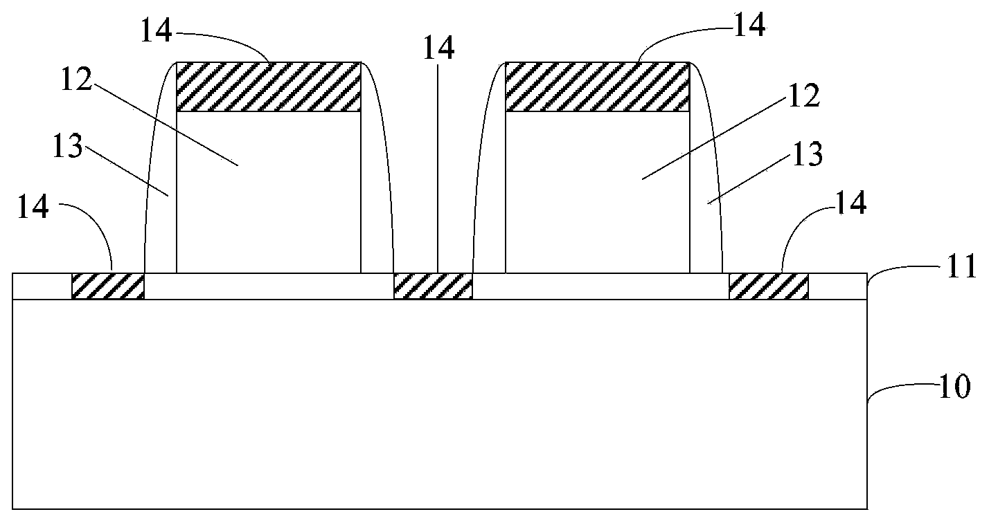
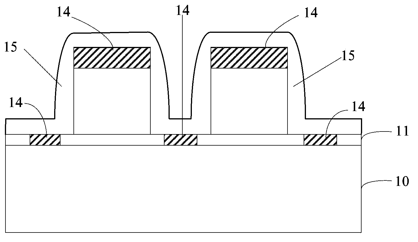
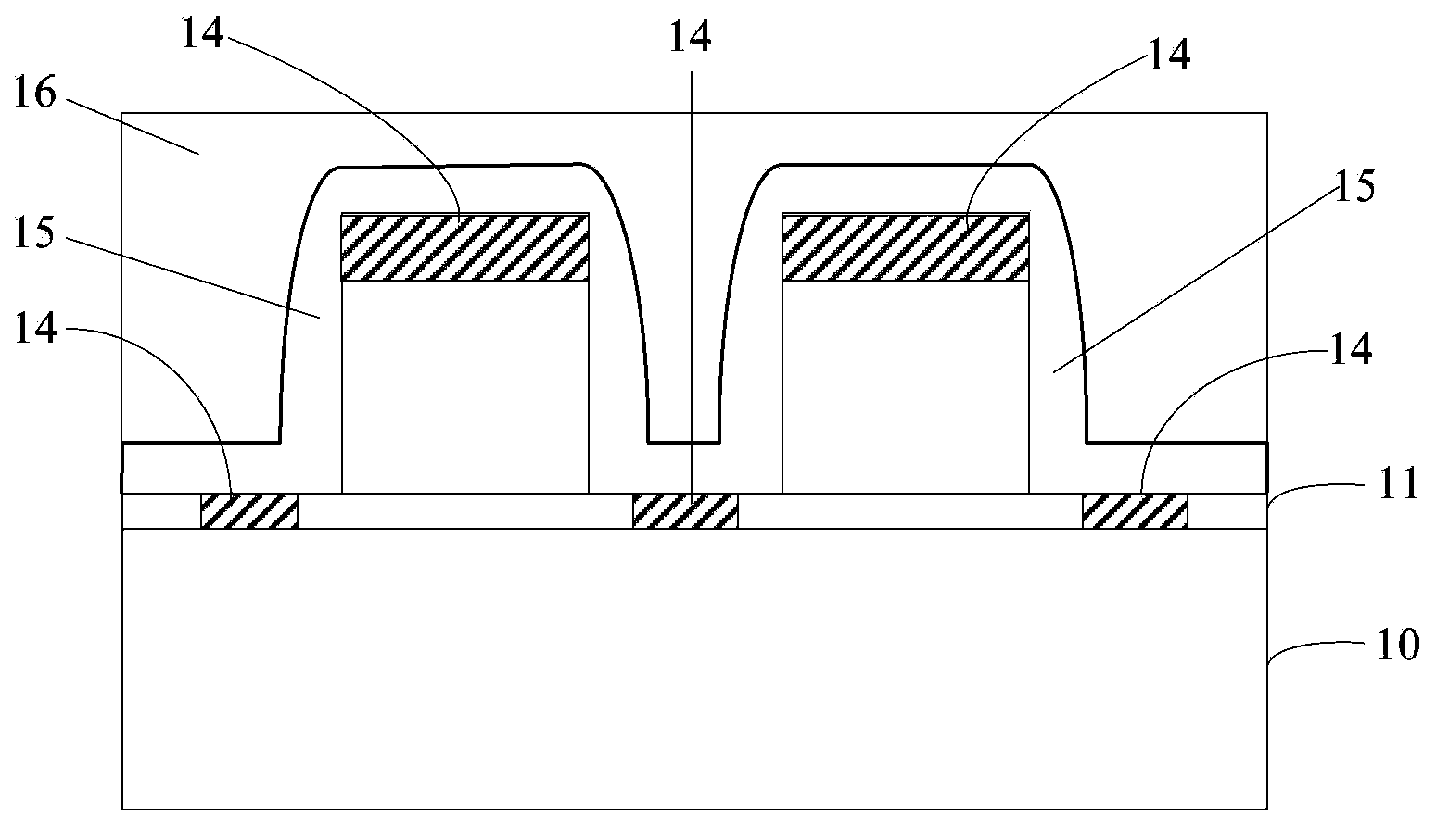
[0044] The inventor analyzed the formation method of the conductive plug in the prior art, and found that: in the process of forming the contact hole, during the process of etching the interlayer dielectric layer and the stress layer by using the ashing process, a polymer will be formed in the contact hole , so after the contact hole is formed, the contact hole needs to be cleaned to remove the polymer. However, the H typically used in the cleaning process 2 SO 4 and H 2 o 2 The mixed solution (SPM) will corrode the side wall of the stress layer. Especially when the material of the stress layer is diamond-like carbon, the SPM acidic solution will corrode the sidewall of the diamond-like carbon stress layer. When the sidewall of the stress layer is corroded, there will be direct contact between the gate and the conductive material in the contact hole, resulting in a short circuit between the gate and the conductive material in the adjacent contact hole, which will inevitabl...


PUM

PropertyMeasurementUnit
Thicknessaaaaaaaaaa

Abstract

The invention discloses an electric conducting plug and a forming method of the electric conducting plug. The forming method of the electric conducting plug comprises the steps that a semiconductor substrate is provided, a grid electrode is formed on the semiconductor substrate, a source region and a drain region are formed in the semiconductor substrate located on the two sides of the grid electrode respectively, a stress layer and an interlayer dielectric layer on the stress layer are formed on the semiconductor substrate, and the stress layer covers the grid electrode, the source region and the drain region; contact holes are formed in the interlayer dielectric layer and the stress layer; a liner layer is formed on the side walls of the contact holes; after the liner layer is formed, the contact holes are cleaned so as to eliminate polymers generated in the process that the contact holes are formed, the liner layer is used for preventing the stress layer from being corroded in the cleaning process of the contact holes, after the contact holes are formed, electric conducting materials are deposited in the contact holes, and the electric conducting plug is formed. Due to the liner layer, the stress layer is prevented from being corroded in the process that the polymers in the contact holes are cleaned later, contact of the grid electrode and the electric conducting plug is further prevented, and good performance of a semiconductor is guaranteed.

Description

technical field [0001] The invention relates to the technical field of semiconductors, in particular to a conductive plug and a method for forming the conductive plug. Background technique [0002] The method for forming conductive plug in prior art: refer to figure 1 , providing a semiconductor substrate 10, on which a gate dielectric layer 11, a gate 12, and sidewalls 13 around the gate 12 are sequentially formed; on the semiconductor substrate 10, a source region and a drain region (not shown) are formed shown); see figure 1 , form a metal silicide (Silicide) 14 on the gate 12, the source region and the drain region, such as nickel silicide (Ni 2 Si); refer to figure 2 , use stress proximity technology (Stress Proximity Technology, SPT) to remove side wall 13; continue to refer to figure 2 , forming a stress layer 15 on the semiconductor substrate 10, the material of the stress layer 15 is silicon nitride; refer to image 3 , forming an interlayer dielectric layer ...

Claims


Application Information

Patent Timeline
IPC IPC(8): H01L23/48H01L21/768
Inventor 韩秋华黄敬勇
Owner SEMICON MFG INT (SHANGHAI) CORP
Why Eureka
Try Eureka