Organic thin-film transistor and manufacturing method thereof

An organic thin film and transistor technology, applied in the field of organic thin film transistors, can solve problems such as poor bias stability, high electrical performance, and difficult production, and achieve high bias stability, high mobility, and stable electrical performance.

Inactive Publication Date: 2014-04-16
HEFEI UNIV OF TECH
View PDF3 Cites 7 Cited by
  • Summary
  • Abstract
  • Description
  • Claims
  • Application Information

AI Technical Summary

Problems solved by technology

[0006] The disadvantages of the existing technology are that it is difficult to manufacture using other processes, the bias stability is poor, and it is difficult to obtain high electrical performance

Method used


Image

  • Organic thin-film transistor and manufacturing method thereof
  • Organic thin-film transistor and manufacturing method thereof
  • Organic thin-film transistor and manufacturing method thereof

Examples


Embodiment 1

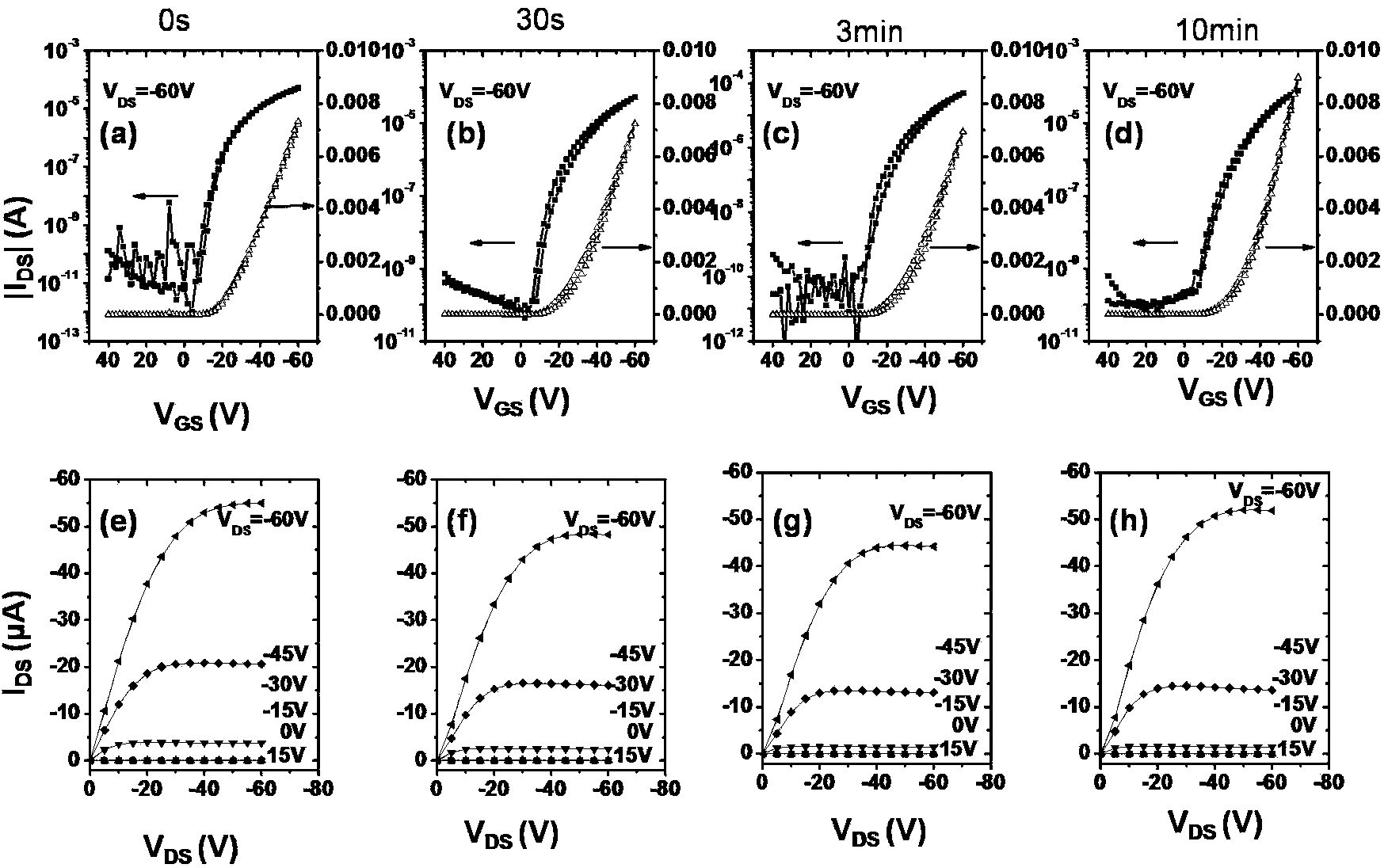
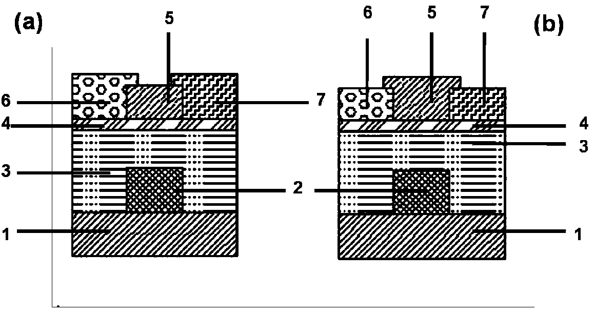
[0045] Such as figure 1As shown, the organic thin film transistor of this embodiment is covered with an insulating layer 3 on a substrate 1 provided with a gate electrode 2, and a surface modification layer 4 is covered on the insulating layer 3, and the surface modification layer 4 is cross-linked after being irradiated with ultraviolet light reaction, an organic semiconductor layer 5 and a source electrode 6 and a drain electrode 7 in ohmic contact with the organic semiconductor layer are provided on the surface modification layer after the crosslinking reaction, and the source electrode 6 and drain electrode 7 are connected through the organic semiconductor layer 5 . figure 1 (a) The semiconductor layer and the source electrode 6 and the drain electrode 7 are in the top contact form, and can also be used figure 1 The bottom contact form shown in (b).

[0046] The organic thin film transistor of this embodiment is prepared according to the following steps:

[0047] a. U...

Embodiment 2

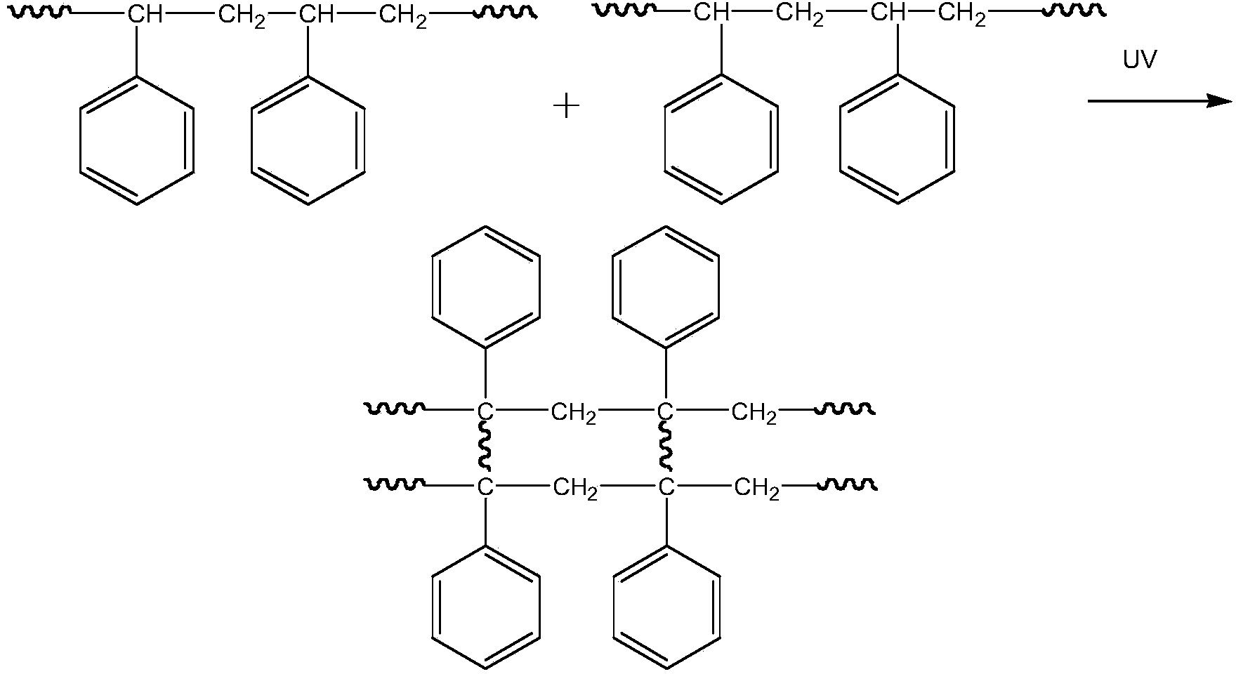
[0058] Polystyrene can be changed into polyvinyl cinnamate, and all the other processing steps are the same as in Example 1.

Embodiment 3

[0060] Polystyrene can be replaced by poly-alpha-methylstyrene material, and the rest of the process steps are the same as in Example 1.


PUM


Abstract

The invention discloses an organic thin-film transistor and a manufacturing method of the organic thin-film transistor. The organic thin-film transistor is characterized in that an insulation layer covers a substrate provided with a grid electrode; a surface decorative layer covers the insulation layer; after the surface decorative layer is illuminated by ultraviolet light, cross-linking reaction is conducted; an organic semiconductor layer, a source electrode and a drain electrode are arranged on the surface decorative layer after the cross-linking reaction is finished, wherein the organic semiconductor layer, the source electrode and the drain electrode are in ohmic contact with the organic semiconductor layer; the source electrode and the drain electrode are communicated through the organic semiconductor layer. According to the organic thin-film transistor, the surface decorative layer is illuminated by the ultraviolet light, so that the cross-linking reaction is conducted on macromolecular polymer; the macromolecular polymer interface decorative layer is additionally arranged between the semiconductor layer and the grid insulation layer, so that a carrier trap of a hydroxide radical group on the grid insulation layer is avoided, the good device performance is obtained, and the hysteresis effect is greatly reduced.

Description

technical field [0001] The invention relates to an organic thin film transistor and belongs to the field of semiconductor devices. Background technique [0002] Organic Thin Film Transistor (OTFT for short) is a semiconductor device that uses organic materials instead of traditional silicon semiconductor materials. Compared with silicon-based materials, organic materials are difficult to process and cost high, but organic thin-film transistors (OTFT) have a very large application in flat-panel displays because of their advantages such as low cost, light weight, low-temperature processing, and suitable for making flexible display devices. Foreground, therefore by the attention of scientific research workers. Since the birth of the first organic thin film transistor in 1987, great progress has been made in the research on OTFT insulating materials, semiconductor materials, electrode materials, and the improvement of device structure. Among the many factors affecting the perf...

Claims


Application Information

Patent Timeline
Patent Type & Authority Applications(China)
IPC IPC(8): H01L51/10H01L51/40
CPCH10K10/474H10K10/476
Inventor 邱龙臻林广庆李鹏朱闵陈梦婕王迎陆红波吕国强
Owner HEFEI UNIV OF TECH
Why Eureka
Try Eureka