Deep sub-micron device sample for in-situ transmission electron microscope and preparation method of sample

An electron microscope, deep submicron technology, applied in the preparation of test samples, etc., can solve problems such as limiting research efficiency and limiting nanoscale device research, and achieve the effect of improving experimental efficiency.

Active Publication Date: 2014-04-23
SOUTHEAST UNIV
View PDF4 Cites 28 Cited by
  • Summary
  • Abstract
  • Description
  • Claims
  • Application Information

AI Technical Summary

Problems solved by technology

However, current TEM samples prepared by focused ion beam systems are usually several microns wide, and a sample can only contain one device, which will limit research efficiency and limit nanoscale device research
How to prepare in situ TEM samples containing multiple, discrete, regular shapes, widths less than 20 nm, and thickness less than 100 nm remains a great challenge

Method used


Image

  • Deep sub-micron device sample for in-situ transmission electron microscope and preparation method of sample
  • Deep sub-micron device sample for in-situ transmission electron microscope and preparation method of sample
  • Deep sub-micron device sample for in-situ transmission electron microscope and preparation method of sample

Examples


Embodiment Construction

[0045] The present invention will be further described below in conjunction with the accompanying drawings.

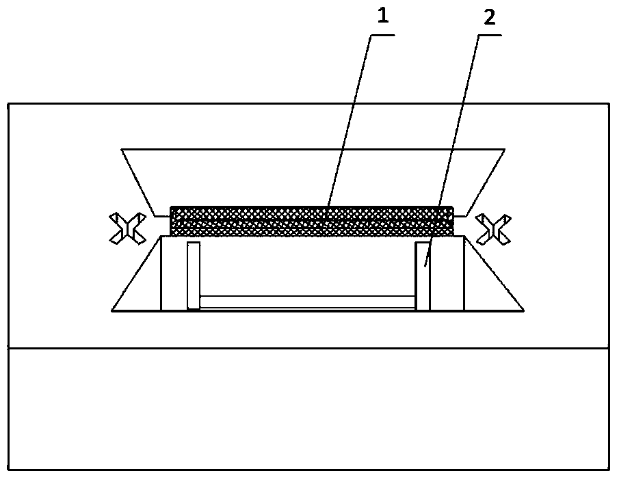
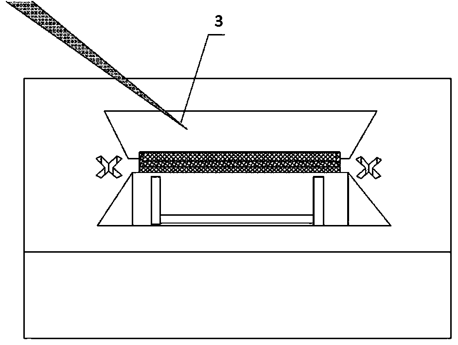
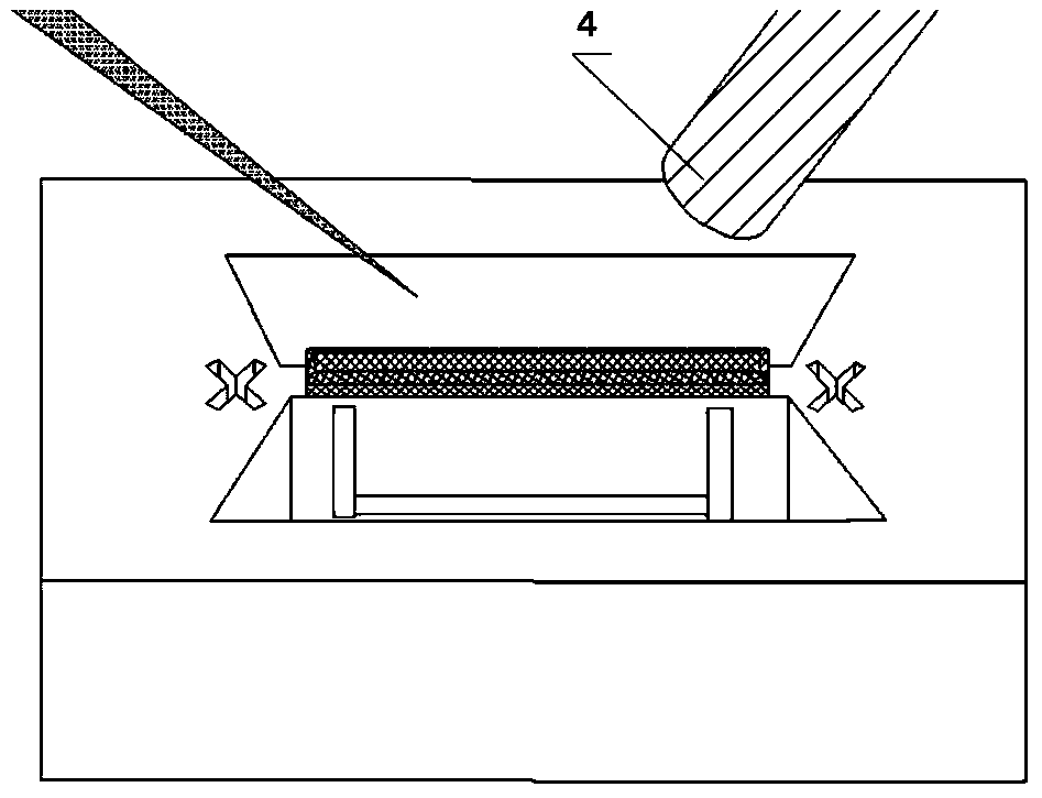
[0046] Figure 1-Figure 8 It is a schematic flow chart of an embodiment of a deep submicron device sample preparation method for in-situ transmission electron microscopy, where the labels are: platinum protective layer 1, "U"-shaped cut 2, mechanical manipulation arm 3, platinum ion gas source detector Needle 4, deposited platinum ions 5, preprocessed transmission electron microscope slice 6, special copper mesh for focused ion beam sample preparation 7, deposited platinum ions 8, containing multiple, discrete, regular shape, width less than 20 nanometers, thickness less than 100 nanometers In situ TEM samples of nanometers 9 .

[0047] Step 1: As shown in Figure (1), first deposit a platinum protective layer 1 with a thickness of ~1 micron on the area of ​​interest of the bulk sample (the part where the TEM thin section sample is made), and use the sample stage to ti...


PUM

PropertyMeasurementUnit
widthaaaaaaaaaa
thicknessaaaaaaaaaa

Abstract

The invention discloses a method for preparing a deep sub-micron device sample for an in-situ transmission electron microscope. Ion beams are focused into ion beams with a small size for performing microdissection or grinding by utilizing an electromagnetic lens by adopting a focused ion beam system, accurate positioning sample preparation can be performed, and a deep sub-micron device is obtained. The method comprises the following steps: cutting and thinning the sample by adopting the focused ion beams so as to obtain a thinned sample, inclining a sample stage at 52+ / -(0.5-1.5) degrees relative to the finally thinned sample through conventional focused ion beams, and innovatively inclining the sample stage at 52+ / -7 degrees. The invention also provides a deep sub-micron device sample for the in-situ transmission electron microscope. The sample comprises multiple discrete nano devices which are regular in shape and have the width of less than 20nm and the thickness of less than 100nm. The sample is suitable for research on the in-situ transmission electron microscope and has the high significance in research on the performance of the deep sub-micron device.

Description

technical field [0001] The invention relates to the fields of semiconductor manufacturing technology and material analysis, in particular to a deep submicron device sample and a preparation method for an in-situ transmission electron microscope. Background technique [0002] Driven by Moore's Law, people pursue integrated circuit technology with higher integration and smaller feature scale. In 2012, Intel adopted the most advanced 22nm process and revolutionary 3D transistor technology, leading the revolution of semiconductor manufacturing technology. Mainstream semiconductor companies such as Intel are committed to the R&D and production of 14nm technology. At the same time, domestic SMIC is speeding up the production of 32-nanometer technology, and the Institute of Microelectronics of the Chinese Academy of Sciences is working on the research and development of 22-nanometer CMOS transistors. With the rapid development of semiconductor manufacturing technology, there is a...

Claims


Application Information

Patent Timeline
Patent Type & Authority Applications(China)
IPC IPC(8): G01N1/28
Inventor 吴幸杨庆龄李斯佳余开浩孙立涛
Owner SOUTHEAST UNIV
Why Eureka
Try Eureka