Sputtering thin film forming device
A technology of sputtering thin films and configuration chambers, which is applied in sputtering plating, ion implantation plating, coating, etc., can solve the problems of reduced film forming speed, reduced plasma density, and difficult formation of oxide films, etc., and achieves improved Density, the effect of increasing the film production speed
- Summary
- Abstract
- Description
- Claims
- Application Information
AI Technical Summary
Problems solved by technology
Method used
Image
Examples
Embodiment 1)
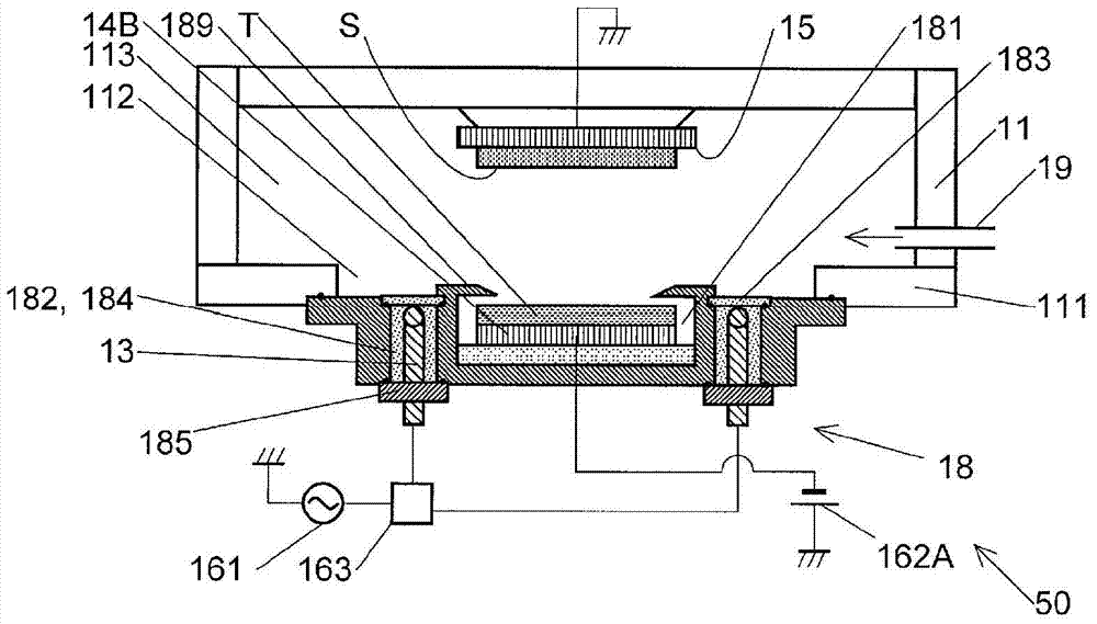
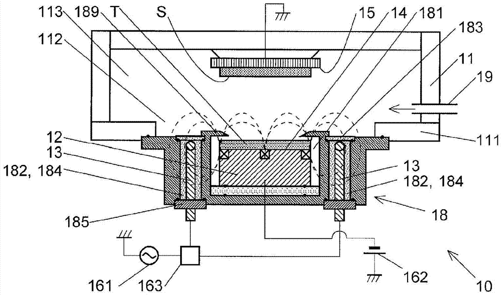
[0046] use figure 1 and figure 2 , the sputtering thin film forming apparatus 10 of the first embodiment will be described. This sputtering thin film forming apparatus 10 is an apparatus that sputters a rectangular plate-shaped target T using plasma to form a predetermined thin film on the surface of a substrate S. As shown in FIG.
[0047] The sputtering thin film forming apparatus 10 has a vacuum container 11, which can make the inside vacuum by using a vacuum pump (not shown); a plasma generating gas introduction part 19, which is used to introduce plasma generating gas into the vacuum container; magnetron sputtering Shooting magnet 12, it is arranged on the bottom of vacuum container 11 as shown in the following; High-frequency antenna 13, it is arranged on the bottom of vacuum container 11 as shown in later; Target base 14, it is arranged on magnetron sputtering the upper surface of the magnet 12; and the substrate holder 15, which is disposed opposite to the target ho...
Embodiment 2)
[0062] use image 3 , the sputtering thin film forming apparatus 20 of the second embodiment will be described. The sputtering thin film forming apparatus 20 of this embodiment is an apparatus for sputtering a rectangular target corresponding to the shape of the substrate in order to form a thin film on the rectangular substrate. In this sputtering thin film forming apparatus 20 , the upper surface of the magnet 12A for magnetron sputtering and the target holder 14A are also rectangular to correspond to the rectangular target. 182 A of radio-frequency antenna arrangement|positioning chambers are provided in both sides of the long side of the magnet 12A for magnetron sputtering, and have the shape extended along the long side direction. A rectangle corresponding to the shape of the high-frequency antenna arrangement chamber 182A is used for the dielectric window 183A. In 182 A of radio-frequency antenna arrangement rooms, a plurality of (in this example, 4 per room) radio-fre...
Embodiment 3)
[0066] use Figure 5 , the sputtering thin film forming apparatus 30 of the third embodiment will be described. In the sputtering thin film forming apparatus 30 of the present embodiment, an exhaust pipe 186 for making the inside of the high-frequency antenna arrangement chamber 182A vacuum is provided in the cover 185A instead of the sputtering thin film forming apparatus 10 of the first embodiment. Dielectric system fill material 184 . Therefore, since the high-frequency antenna arrangement chamber 182A is also vacuumed in addition to the internal space 113 of the vacuum container 11 , it is possible to more efficiently generate a high-frequency induction electric field in the internal space 113 . In addition, since there is no pressure difference between the front and rear sides of the dielectric window 183, the mechanical strength of the dielectric window 183 does not become a problem, and the thickness of the dielectric window 183 can be reduced, and the protection of th...
PUM
 Abstract
Description
Claims
Application Information


