

SiC epitaxial wafer and method for manufacturing same
A technology for epitaxial wafers and manufacturing methods, which is applied in chemical instruments and methods, semiconductor/solid-state device manufacturing, crystal growth, etc., and can solve problems such as the expansion of lamination defect areas
- Summary
- Abstract
- Description
- Claims
- Application Information
AI Technical Summary
Problems solved by technology
Method used
Image

Examples
no. 1 Embodiment approach )
[0064] The method of manufacturing a SiC epitaxial wafer according to the first embodiment of the present invention is a method of manufacturing a SiC epitaxial wafer provided with an SiC epitaxial layer on a SiC single crystal substrate having an off angle, and is characterized in that it includes: Among the basal plane dislocations (BPD) existing in the growth plane of the SiC single crystal substrate, the process of determining the ratio of stacking defects in the SiC epitaxial film of a predetermined film thickness formed on the SiC single crystal substrate; based on the ratio, determine The process of using the upper limit of the BPD area density in the growth surface of the SiC single crystal substrate; and using the SiC single crystal substrate below the upper limit, under the same conditions as the growth conditions of the epitaxial film used in the process of determining the ratio, on the SiC single crystal substrate The process of forming a SiC epitaxial film on a cry...
no. 2 Embodiment approach )
[0127] A method of manufacturing a SiC epitaxial wafer according to a second embodiment of the present invention is a method of manufacturing a SiC epitaxial wafer provided with an SiC epitaxial layer on a SiC single crystal substrate having an off angle, and is characterized in that: Among the basal plane dislocations (BPD) and threading screw dislocations (TSD) existing in the growth plane of the SiC single crystal substrate, the ratio of carrot defects in the SiC epitaxial film with a predetermined film thickness formed on the SiC single crystal substrate process; a process of determining the upper limit of the areal density of the BPD of the growth surface of the SiC single crystal substrate used based on the ratio; and using the SiC single crystal substrate below the upper limit so as to be the same as the growth conditions of the epitaxial film used in the process of determining the ratio conditions, the process of forming a SiC epitaxial film on a SiC single crystal subs...
Embodiment 1)
[0148] A SiC epitaxial wafer in which a SiC epitaxial layer was formed on the Si surface of a 4H-SiC single crystal substrate inclined at an off angle of 4° was produced.
[0149] In this example, no convex processing was performed on the 4H-SiC single crystal substrate.
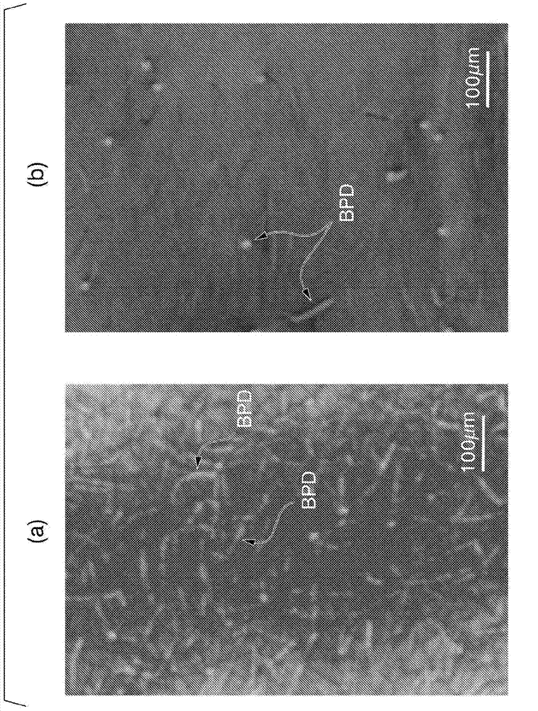
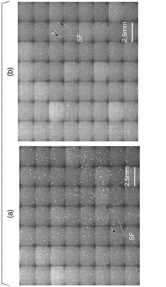
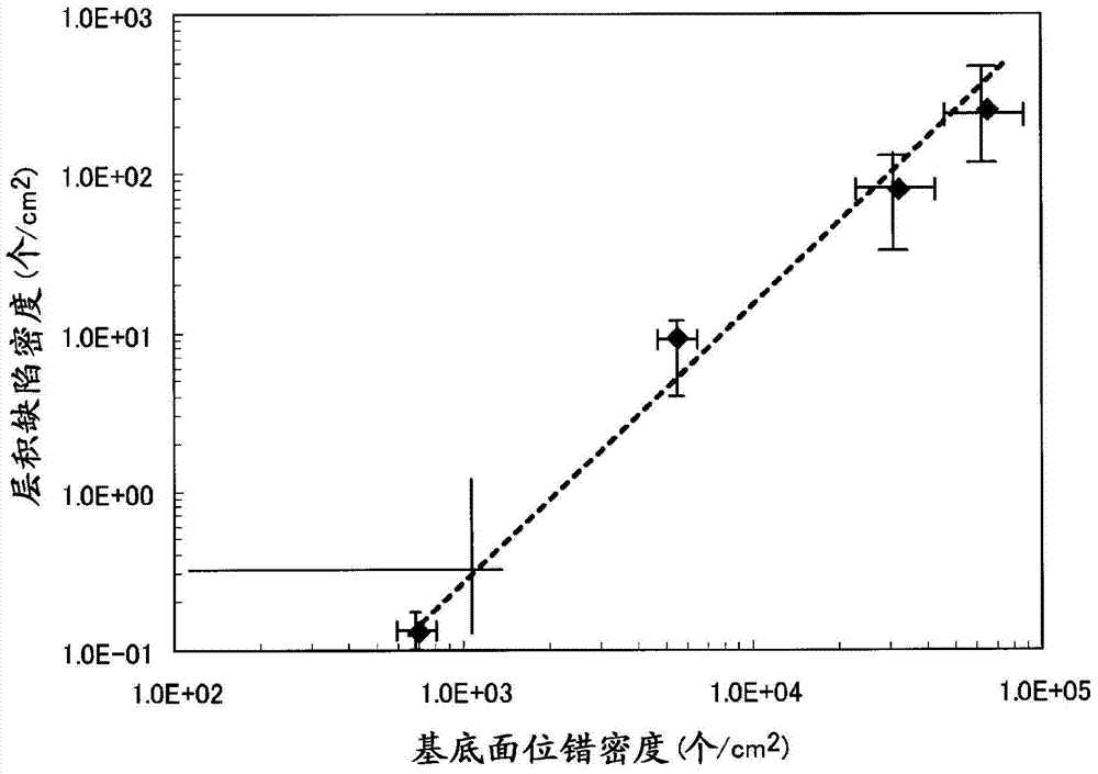
[0150] First, four SiC single crystal substrates were polished under four polishing conditions in order to determine the conversion efficiency to stacking defects (SF). The areal densities of the four basal plane dislocations (BPDs) shown in Table 1 correspond to the areal densities of the basal plane dislocations (BPDs) of the SiC single crystal substrates polished under these polishing conditions.
[0151] In addition, the one with the lowest BPD density was performed under the following polishing conditions. That is, the mechanical polishing before CMP uses abrasive grains with a diameter of 5 μm or less, and the processing pressure is 350 g / cm 2 to proceed. In addition, CMP was performed for 30 minute...
PUM
| Property | Measurement | Unit |
|---|---|---|
| The average particle size | aaaaa | aaaaa |
Abstract
Description
Claims
Application Information