Cu-Ni-Si alloy and method for manufacturing same

A cu-ni-si, manufacturing method technology, applied in the direction of metal/alloy conductors, conductive materials, conductive materials, etc., can solve the problems of local punching and processing deepening, and achieve the effect of excellent strength

Inactive Publication Date: 2014-05-07
JX NIPPON MINING & METALS CO LTD
View PDF6 Cites 18 Cited by
  • Summary
  • Abstract
  • Description
  • Claims
  • Application Information

AI Technical Summary

Problems solved by technology

With the miniaturization of products, there is a tendency to deepen the local punching process in order to further improve the shape accuracy of the terminal

Method used


Image

  • Cu-Ni-Si alloy and method for manufacturing same
  • Cu-Ni-Si alloy and method for manufacturing same
  • Cu-Ni-Si alloy and method for manufacturing same

Examples


Embodiment 1)

[0084] An alloy containing Ni: 2.6% by mass, Si: 0.58% by mass, Sn: 0.5% by mass, and Zn: 0.4% by mass, and the remainder consisting of copper and unavoidable impurities was used as an experimental material. The relationship between the processing degree of cold rolling and the strain rate of the third cold rolling, crystal orientation and n value, and the influence of crystal orientation and n value on product bendability were studied.

[0085]2.5 kg of electrolytic copper was melted in a high-frequency melting furnace in an argon atmosphere using a graphite crucible with an inner diameter of 60 mm and a depth of 200 mm. Alloying elements were added to obtain the above-mentioned alloy composition, and the temperature of the melt was adjusted to 1300° C., followed by casting in a cast iron mold to form an ingot with a thickness of 30 mm, a width of 60 mm, and a length of 120 mm. This ingot was heated at 950° C. for 3 hours, and hot rolled to a thickness of 10 mm. Use a grinde...

Embodiment 2)

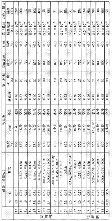
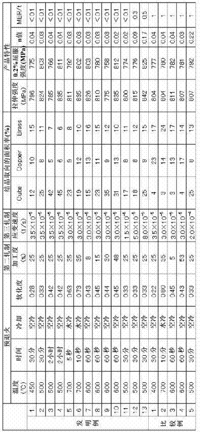
[0110] Whether or not the improvement effect of bendability shown in Example 1 can be obtained by Cu—Ni—Si alloys having different compositions and manufacturing conditions was examined.

[0111] Casting, hot rolling, and surface grinding were carried out in the same manner as in Example 1 to obtain a plate having a thickness of 9 mm having the composition shown in Table 2. This plate was rolled and heat-treated in the following order of steps to produce a product sample with a plate thickness of 0.15 mm.

[0112] (1) First cold rolling: cold rolling to a predetermined thickness corresponding to the rolling degree of the second cold rolling.

[0113] (2) Pre-annealing: Insert the sample into an electric furnace adjusted to a specified temperature, and after keeping it for a specified time, cool it under the following two conditions: put the sample in a water tank for cooling (water cooling), or place the sample in a Cooling in the atmosphere (air cooling).

[0114] (3) Secon...


PUM

PropertyMeasurementUnit
tensile strengthaaaaaaaaaa
yield strengthaaaaaaaaaa
Area ratioaaaaaaaaaa

Abstract

Provided is a Cu-Ni-Si alloy and a method for manufacturing the Cu-Ni-Si alloy, the Cu-Ni-Si alloy being provided with exceptional strength and bendability, and being suitable as an electro-conductive spring material for a connector, terminal, relay, switch or other component. The Cu-Ni-Si alloy contains 1.0 to 4.5 wt% of Ni, 0.2 to 1.0 wt% of Si, and copper and inevitable impurities constituting the balance. Electron back-scatter diffraction (EBSD) measuring is performed. When the crystal orientation is analyzed the area of cube orientation {001} <100>; constitutes 5% or more, the area of brass orientation {110} <112>; constitutes 20% or less, and the area of copper orientation {112} <111>; constitutes 20% or less. The work-hardening coefficient is 0.2 or less.

Description

technical field [0001] The present invention relates to a copper alloy having excellent strength and bending workability, which is suitable as a conductive spring material for connectors, terminals, relays, switches, etc., and a method for producing the same. Background technique [0002] In recent years, along with the miniaturization of electronic equipment, the miniaturization of electrical and electronic components has been progressing. Furthermore, copper alloys used for these components are required to have good strength and electrical conductivity. [0003] Copper alloys used in automotive terminals are also required to have good strength and electrical conductivity along with miniaturization. Furthermore, in many automotive receptacle terminals, a notching process called notching process is performed on the bent inner surface before the press bending process. This is processing to improve shape accuracy after press bending. Along with product miniaturization, ther...

Claims


Application Information

Patent Timeline
Patent Type & Authority Applications(China)
IPC IPC(8): C22C9/06C22C9/00C22C9/01C22C9/02C22C9/04C22C9/05C22C9/10C22F1/08H01B1/02C22F1/00
CPCC22F1/08C22C9/06H01B1/026
Inventor 长野真之
Owner JX NIPPON MINING & METALS CO LTD
Why Eureka
Try Eureka