Method for removing transition metal impurities in silicon wafer or silicon device in sucking mode at indoor temperature

A technology of transition metals and silicon wafers, applied in semiconductor/solid-state device manufacturing, electrical components, circuits, etc., can solve problems such as destroying device structures

Active Publication Date: 2014-05-14
PEKING UNIV
View PDF5 Cites 15 Cited by
  • Summary
  • Abstract
  • Description
  • Claims
  • Application Information

AI Technical Summary

Problems solved by technology

[0003] Usually gettering methods (such as back damage, phosphorus diffusion, and aluminum alloys, etc.) require high temperatures of five to six hundred or even thousands of degrees Celsius for tens of minutes to ten hours. Such long-term high temperatures are likely to damage the device structure.

Method used


Image

  • Method for removing transition metal impurities in silicon wafer or silicon device in sucking mode at indoor temperature
  • Method for removing transition metal impurities in silicon wafer or silicon device in sucking mode at indoor temperature
  • Method for removing transition metal impurities in silicon wafer or silicon device in sucking mode at indoor temperature

Examples


Embodiment 1

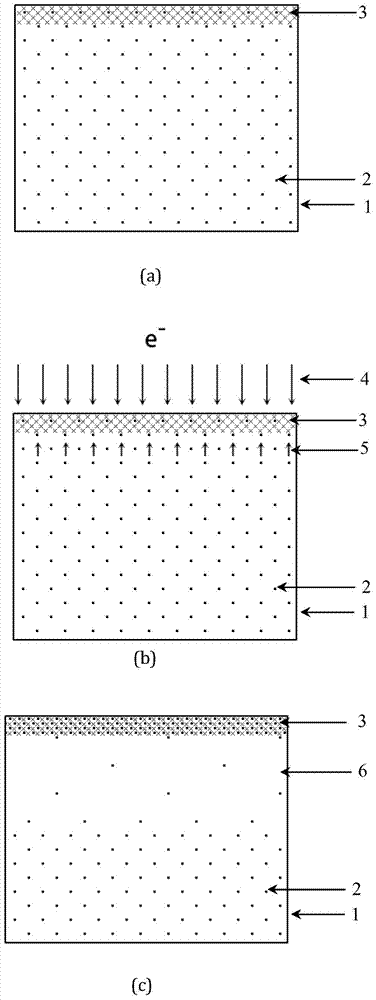
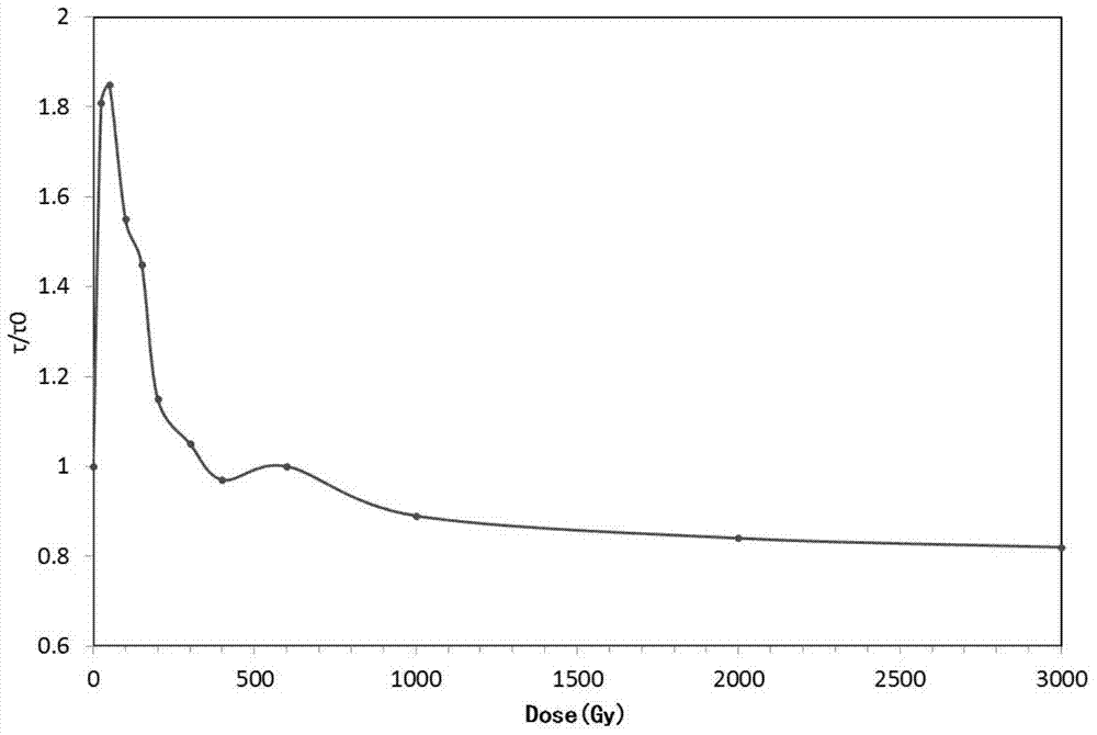
[0020] Gold is injected into the polished silicon single wafer sample, and the transition metal impurity gold in the silicon wafer is removed by electron irradiation gettering method, and the effect of electron irradiation gettering is measured. Specifically, the ion implantation method is used to implant gold, the implantation energy is 550KeV, and the surface density is 1×10 12 cm -2, A silicon single wafer containing transition metal impurity gold was obtained for gettering experiments. Before gettering, use ICP (inductively coupled plasma) equipment to process the silicon single wafer for 2 minutes at a power of 250W, and introduce new defect regions with a depth of no more than 20 nanometers on the front surface of the silicon single wafer. Then use an electron accelerator to irradiate the front side of the silicon wafer at an energy of 3-5 MeV, and the radiation dose rate is about 8Gy / s, τ / τ 0 as a function of radiation dose figure 2 shown. When the irradiation dose...

Embodiment 2

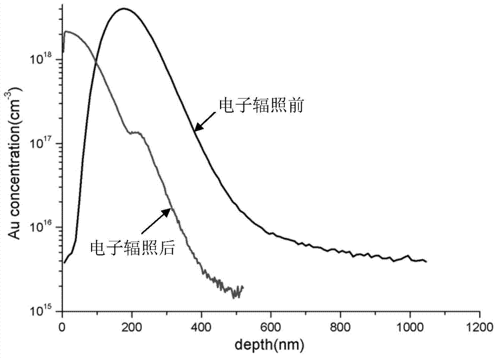
[0022] Gold is injected into the polished silicon single wafer sample, and the gold implanted in the silicon wafer is removed by electron radiation gettering method to detect the effect of electron radiation gettering. Specifically, the ion implantation method is used to implant gold, the implantation energy is 550KeV, and the surface density is 7×10 13 cm -2 . Using the gettering method and condition parameters in the above-mentioned embodiment 1, SIMS (secondary ion mass spectrometry) measures the distribution of gold on the silicon single wafer before and after electron irradiation, and the distribution peak of the impurity gold that was originally in the area to be cleaned is obviously towards the silicon wafer. The gettering defect region on the surface moves, such as image 3 shown. The gettering effect of the transition metal impurity Au diffusing to the gettering defect region and being trapped under electron irradiation was confirmed.

Embodiment 3

[0024] Transition metal impurity gold is injected into the polished silicon single wafer sample, and the effect of absorbing gold in the silicon wafer by room temperature electron irradiation is tested. Specifically, gold is implanted with ions, the energy is 550KeV, and the implantation dose is 1×10 12 cm -2 . Use ICP (Inductively Coupled Plasma) equipment to process the silicon single wafer for 2 minutes at a power of 250W, and introduce a gettering defect region with a depth of no more than 20 nanometers on the front surface. Then use an electron accelerator to irradiate the front of the wafer with an energy of 3-5 MeV, the radiation dose rate is 50Gy / s, and the radiation dose is 200Gy, and measure the ratio τ / τ of the minority carrier lifetime of the sample before and after electron irradiation 0 is 1.96, that is, the minority carrier lifetime is nearly doubled after electron irradiation, reflecting the decrease in the concentration of transition metal gold as a recombin...


PUM


Abstract

The invention discloses a method for removing transition metal impurities in a silicon wafer or silicon device in a sucking mode at the indoor temperature. Low-dose electron irradiation with the dose smaller than 5000 Gy is carried out on the silicon wafer or silicon device at the indoor temperature to enable the transition metal impurities in a to-be-cleaned area of the silicon wafer or an active area of the silicon device to be diffused to a nearby impurity sucking defect area, and therefore the concentration of the transition metal impurities in the to-be-cleaned area of the silicon wafer or the active area of the silicon device is lowered. Compared with an existing silicon material impurity sucking method, the method is implemented at the indoor temperature, and therefore the method can be used for silicon wafer or silicon device impurity sucking, is not limited to the single-crystal or polycrystalline silicon wafer and the silicon device, and is also suitable for other semiconductor materials such as germanium, and corresponding devices.

Description

technical field [0001] The invention relates to a method for removing transition metal impurities in silicon wafers and silicon devices at room temperature, in particular to using low-dose electron irradiation and gettering defect regions to get rid of transition metal impurities in silicon wafers or silicon devices at room temperature, thereby improving Methods of silicon wafer quality or silicon device performance. Background technique [0002] Both silicon wafers and silicon devices contain transition metal impurities such as copper, iron, nickel, and gold, and are inevitably contaminated by various transition metal impurities in the process of device preparation. Performance is severely adversely affected. In the process of silicon devices such as large-scale integrated circuits, solar cells, and photodetectors, the content of transition metal impurities should be reduced as much as possible. Gettering technology is usually used in combination with a reasonable process...

Claims


Application Information

Patent Timeline
Patent Type & Authority Applications(China)
IPC IPC(8): H01L21/02H01L21/265
CPCH01L21/2636H01L21/322H01L21/3221
Inventor 徐万劲秦国刚张瑜秦来香
Owner PEKING UNIV
Why Eureka
Try Eureka