Method for Improving Edge Roughness of Tungsten Silicide Double Gate of Self-Aligned Contact Hole

A self-aligned contact hole and edge roughness technology, which is applied in the direction of electrical components, semiconductor/solid-state device manufacturing, semiconductor devices, etc., can solve the problems of large tungsten silicide grains and inclined morphology, and achieve improved edge roughness, Avoid etch residue, the effect of smooth gate sidewall

Active Publication Date: 2016-08-17
SHANGHAI HUAHONG GRACE SEMICON MFG CORP
View PDF6 Cites 0 Cited by
  • Summary
  • Abstract
  • Description
  • Claims
  • Application Information

AI Technical Summary

Problems solved by technology

Due to the limitation of the amount of etching and the large tungsten silicide grains, the first step of etching the bottom of tungsten silicide is easy to form a tilted shape.

Method used


Image

  • Method for Improving Edge Roughness of Tungsten Silicide Double Gate of Self-Aligned Contact Hole
  • Method for Improving Edge Roughness of Tungsten Silicide Double Gate of Self-Aligned Contact Hole
  • Method for Improving Edge Roughness of Tungsten Silicide Double Gate of Self-Aligned Contact Hole

Examples


Embodiment Construction

[0029] The present invention will be described in further detail below in conjunction with the accompanying drawings and embodiments.

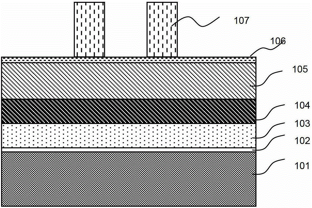
[0030] figure 1 Fig. 5 has shown processing steps of the present invention, and the inventive method mainly comprises the following steps:

[0031] 1. If figure 1 As shown, a gate dielectric layer 102 (a gate oxide film is used in this embodiment) with a thickness of 20-40 angstroms is grown on a silicon substrate 101 by thermal oxidation; on the gate dielectric layer, a CVD method is used to deposit A layer of polysilicon 103 of about 700-800 angstroms, polysilicon deposition temperature is selected at 500-600 degrees Celsius, CVD or PVD is used to grow tungsten silicide (WSix) 104 on the polysilicon 103, the thickness is 600-750 angstroms, and the process temperature of CVD and PVD can not exceed 600 degrees Celsius, so as to avoid the formation of silicon clusters in WSix; on the tungsten silicide 104, use PECVD or CVD process to deposi...


PUM

PropertyMeasurementUnit
thicknessaaaaaaaaaa
thicknessaaaaaaaaaa
thicknessaaaaaaaaaa

Abstract

The invention discloses a method for improving tungsten silicide bigrid edge roughness of a self-aligning contact hole. The method comprises the following steps: 1.1 a tungsten silicide grid pattern is formed; 1.2 first time of grid etching is performed on tungsten silicide grid; 1.3 photo-resist is removed by adopting dry etching with a function of modifying morphology of the side wall of tungsten silicide, and then cleaning is performed by adding pure water to rinse; 1.4 dielectric film silicon nitride is deposited; and 1.5 second time of grid etching is performed and residual polycrystalline silicon is etched. In the step of photo-resist removing after completion of first time of etching, a special step of photo-resist removing with carbon tetrafluoride, which is different from a conventional step of photo-resist removing by oxygen, is adopted, and rinsing processing is performed by adding pure water. Partial side wall of tungsten silicide can be etched by the special step of photo-resist removing with carbon tetrafluoride, and the side wall of the tungsten silicide film layer can be modified to be vertical in morphology so that a small dielectric film blocking wall is difficult to form in the subsequent dielectric film deposition and second step of etching, and thus residual in polycrystalline silicon etching can be avoided.

Description

technical field [0001] The invention belongs to a manufacturing process method of a semiconductor integrated circuit, and in particular relates to a method for automatic cleaning of ion implantation equipment, in particular to a method for automatic cleaning of an ion cavity of ion implantation equipment to improve the service life of components. Background technique [0002] The tungsten silicide double gate structure of the self-aligned contact hole uses a multi-layer gate structure of silicon nitride, tungsten silicide, and polysilicon structure. The device has the characteristics of small device area and low production cost, and is widely used in SIM cards and financial cards. And MCU SOC product manufacturing. [0003] In the tungsten silicide double-gate device with self-aligned contact holes, in order to solve the short circuit problem of the self-aligned contact hole to the gate, the traditional gate etching process usually needs to be etched in two steps: the first ...

Claims


Application Information

Patent Timeline
Patent Type & Authority Patents(China)
IPC IPC(8): H01L21/28
CPCH01L21/28H01L21/76897
Inventor 孙娟郁新举吴智勇
Owner SHANGHAI HUAHONG GRACE SEMICON MFG CORP
Why Eureka
Try Eureka