Manufacturing method of composite substrate structure used for nitride growth

A technology of a composite substrate and a manufacturing method, which is applied to electrical components, circuits, semiconductor devices, etc., can solve problems such as the limitation of improving the light emitting rate of light-emitting diodes, affecting the brightness of light-emitting diodes, and complex processes.

Inactive Publication Date: 2014-06-04
EPILIGHT TECH
View PDF3 Cites 9 Cited by
  • Summary
  • Abstract
  • Description
  • Claims
  • Application Information

AI Technical Summary

Problems solved by technology

However, for sapphire substrates with raised structures, direct deposition of GaN light-emitting epitaxial structures often brings huge crystal defects, which seriously affects the brightness of light-emitting diodes. H was performed on the surface of the sapphire substrate with the raised structure left and right 2 Reduction treatment, and then the reaction source is introduced, and a low-temperature GaN layer is deposited on the surface of the sapphire substrate by low-temperature chemical vapor deposition, and then the reaction source is stopped, and the temperature is raised to about 1050°C to make th

Method used


Image

  • Manufacturing method of composite substrate structure used for nitride growth
  • Manufacturing method of composite substrate structure used for nitride growth
  • Manufacturing method of composite substrate structure used for nitride growth

Examples


Embodiment 1

[0035] Such as Figure 1 to Figure 7 As shown, this embodiment provides a method for manufacturing a composite substrate structure for nitride growth, which at least includes the following steps:

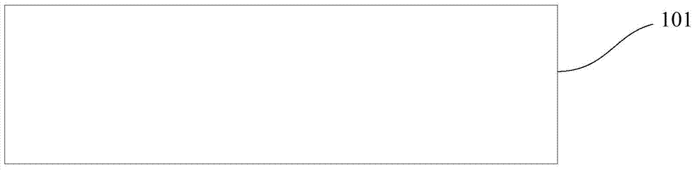
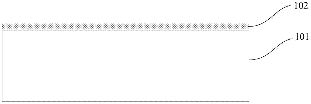
[0036] Such as Figure 1 ~ Figure 2 As shown, step 1) is firstly performed, a growth substrate 101 is provided, and a buffer layer 102 for subsequent growth of a light-emitting epitaxial structure is formed on the surface of the growth substrate 101 .

[0037] As an example, the material of the growth substrate 101 is one of sapphire, SiC, Si and ZnO. In this embodiment, the growth substrate 101 is a flat sapphire substrate with a flat surface. The buffer layer 102 is low-temperature Al prepared by low-temperature chemical vapor deposition. x Ga 1-x N layer (0≤X≤0.5), preferably low temperature Al x Ga 1-x For N layers (0≤X≤0.2), the temperature range for preparation is 450-700°C. In this example, the low temperature Al x Ga 1-x The preparation temperature of the N layer (0≤...

Embodiment 2

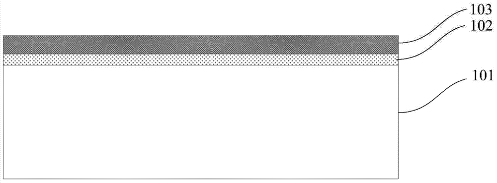
[0049] Such as Figure 1 to Figure 6 and Figure 8 As shown, this embodiment provides a method for manufacturing a composite substrate structure for nitride growth, the basic steps of which are as in Embodiment 1, wherein:

[0050] The buffer layer 102 is an AlN layer prepared by a sputtering method, and the crystal orientation or main crystal orientation of the AlN layer is (0001) orientation. Compared to low temperature Al x Ga 1-x N layer, the advantage of sputtering AlN layer preparation is strong controllability of thickness, high degree of crystal orientation, and it is also conducive to the nucleation and growth of light-emitting epitaxial structures (especially GaN-based light-emitting epitaxial structures).

[0051] As another solution of this embodiment, the buffer layer 102 is a BN material layer prepared by methods such as sputtering.

[0052] Such as Figure 8 As shown, in this embodiment, the plurality of hole structures 106 are arranged in a hexagonal array...


PUM

PropertyMeasurementUnit
Thicknessaaaaaaaaaa
Thicknessaaaaaaaaaa
Apertureaaaaaaaaaa

Abstract

The invention provides a manufacturing method of a composite substrate structure used for nitride growth. The manufacturing method comprises the steps that (1) a buffer layer used for growth of a subsequent luminous epitaxial structure is formed on the surface of a growth substrate; (2) an SiO2 layer is formed on the surface of the buffer layer; (3) a mask layer with a plurality of hole-shaped windows which are arranged at intervals is formed on the surface of the SiO2 layer; (4) the hole-shaped windows are used for etching the SiO2 layer to form a plurality of hole-shaped structures in the SiO2 layer, and the parts, below the hole-shaped structures, of the buffer layer are exposed out. According to the manufacturing method, a BN material layer or an AlN layer or an AlxGal-xN layer with a hexagonal lattice structure is manufactured first to serve as the buffer layer for growth of the luminous epitaxial structure, and then the hole-shaped structures which are arranged at intervals are manufactured in the SiO2 layer through an ICP etching technology. The buffer layer and the SiO2 layer with the hole-shaped structures can guarantee the quality of crystals with grown luminous epitaxial structures, and can also improve the light emitting efficiency of a light-emitting diode. The manufacturing method of the composite substrate structure used for nitride growth is simple in technology, beneficial for lowering the manufacturing cost and applicable to industrial production.

Description

technical field [0001] The invention relates to the field of semiconductor lighting, in particular to a method for manufacturing a composite substrate structure for nitride growth. Background technique [0002] As a new type of high-efficiency solid light source, semiconductor lighting has significant advantages such as long life, energy saving, environmental protection, and safety. It will become another leap in the history of human lighting after incandescent lamps and fluorescent lamps. The upgrading of the industry and other industries has huge economic and social benefits. Because of this, semiconductor lighting is generally regarded as one of the most promising emerging industries in the 21st century, and also one of the most important commanding heights in the field of optoelectronics in the next few years. Light-emitting diodes are made of III-V compounds, such as GaAs (gallium arsenide), GaP (gallium phosphide), GaAsP (gallium arsenide phosphide) and other semicond...

Claims


Application Information

Patent Timeline
IPC IPC(8): H01L33/00H01L33/12H01L33/20
CPCH01L33/0075H01L33/12H01L33/20
Inventor 袁根如郝茂盛邢志刚李振毅陈耀
Owner EPILIGHT TECH
Why Eureka
Try Eureka