Surface treatment method of substrate for solar cell
A solar cell and surface treatment technology, applied in post-processing, post-processing details, chemical instruments and methods, etc., can solve problems such as low light absorption rate and solar cell efficiency reduction, and achieve the effect of simplifying the process and reducing costs
- Summary
- Abstract
- Description
- Claims
- Application Information
AI Technical Summary
Problems solved by technology
Method used
Image
Examples
Embodiment 1
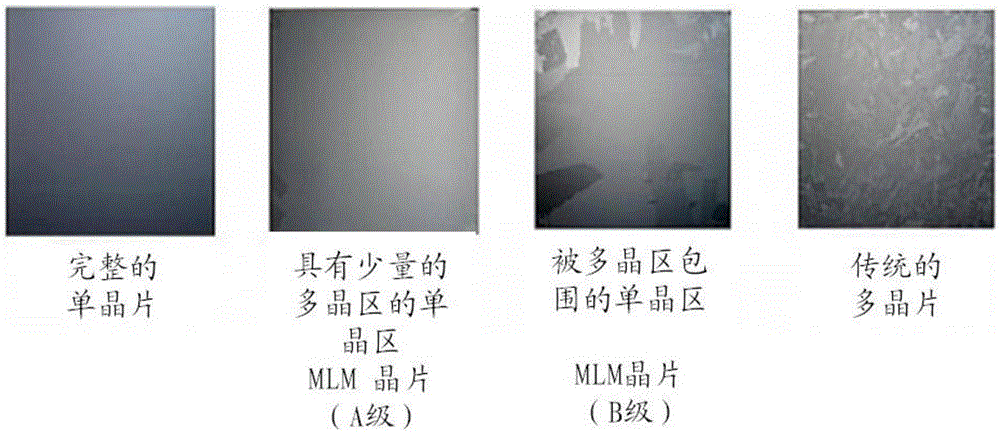
[0080] A p-type quasi-single crystal substrate (MLM wafer, Grade B) doped with group III element impurities is prepared. In the volume ratio of 1:3:2 containing HF, HNO 3 and H 2 In the solution of O, the substrate is immersed for 1 minute and 30 seconds at a temperature of 7° C. to perform the first wet etching, so as to simultaneously perform the cutting damage removal and the first texturing treatment. Through the first texturing treatment, the etching thickness from the surface is 3-5 μm.
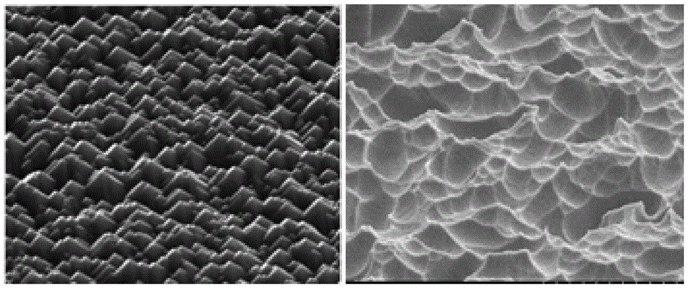
[0081] Then, as etching gas using Cl 2 / SF 6 / O 2 A reactive ion etching process is performed. The ratio H / W of the height (Height) to the width (Width) of the pyramid structure formed by the reactive ion etching process is distributed in the range of 0.75˜1.1.
[0082] In the volume ratio of 1:15:17 containing HF, HNO 3 and H 2 In the solution of O, immerse the substrate for 30 seconds at a temperature of 25°C to perform the second wet etching. After the etching, the weight of ...
experiment example
[0088] Evaluation of Surface Treatment Results
[0089] Figure 4 This is a photograph taken at a 70,000-fold magnification of the surface of the substrate after the reactive ion etching step in Example 1 using a scanning electron microscope.
[0090] Figure 5 This is a photograph of the surface of the substrate after the reactive ion etching process and the second wet etching process in the above-mentioned Example 1 at a magnification of 5000 times and taken with a scanning electron microscope.
[0091] Image 6 It is a graph showing the reflectance of the substrate before the surface treatment and the reflectance of the substrate after the surface treatment process in the above-mentioned Example 1 and Comparative Example 1.
[0092] Electrical Performance Evaluation of Solar Cells
[0093] According to ASTM G-173-03, under AM1.5 light conditions, the photovoltaic tester (solar tester) of Hanwha Solarone Limited (HSOL) in China, that is, H.a.l.m cetis PV-products is ...
PUM
| Property | Measurement | Unit |
|---|---|---|
| height | aaaaa | aaaaa |
| width | aaaaa | aaaaa |
| height | aaaaa | aaaaa |
Abstract
Description
Claims
Application Information


