

Forming method for transistor
A technology of transistors and semiconductors, applied in the manufacture of transistors, semiconductor devices, semiconductor/solid-state devices, etc., can solve problems such as poor performance of transistors, and achieve the effect of improving reliability and performance
- Summary
- Abstract
- Description
- Claims
- Application Information
AI Technical Summary
Problems solved by technology
Method used
Image

Examples
Embodiment Construction
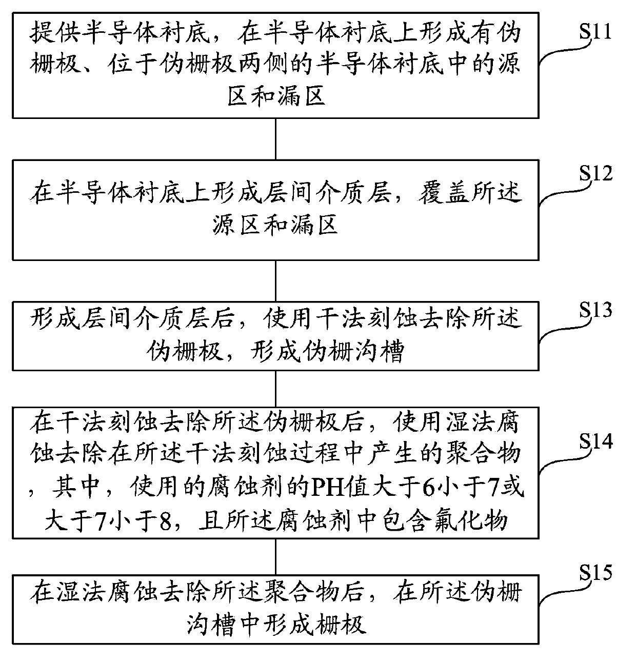
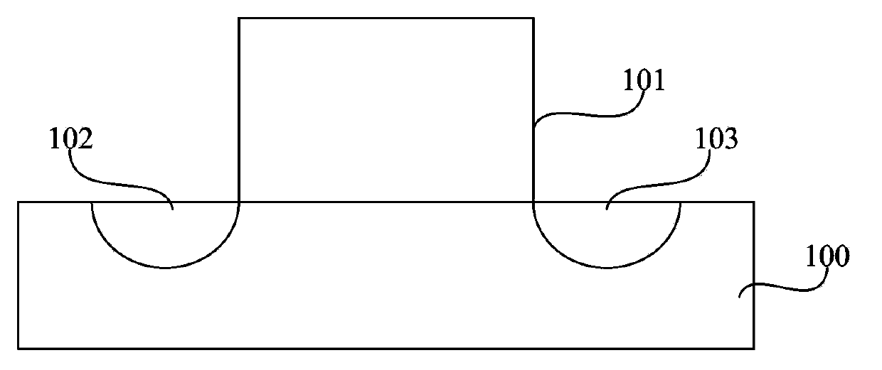
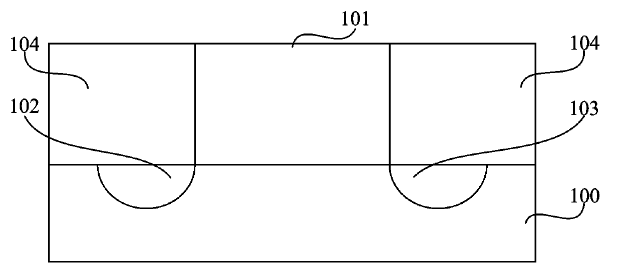
[0040] The inventors conducted research on the problems existing in the gate-last process of the prior art, and found that: in the process of removing the dummy gate by dry etching, polymers will be formed and adhere to the bottom and sidewalls of the dummy gate trench. For example, in the dry etching process, oxygen is usually introduced into the etching reaction chamber, and part of the oxygen will react with polysilicon or other substances in the etching reaction chamber to form oxides, which can be regarded as a kind of polymer Element. Although, subsequent wet etching is used to remove the polymer, the etchant commonly used in the prior art is N-methylpyrrolidone (NMP, N-methyl-2-pyrrolidone) solvent or EKC solvent (a product provided by DuPont EKC Technology Co., Ltd. an alkaline solution). Both NMP solvent and EKC solvent have strong alkalinity. While removing polymers, they also cause damage to adjacent semiconductor devices. The ability of NMP solvents or EKC solvent...
PUM
 Abstract
Description
Claims
Application Information