Organic electroluminescence device and preparing method thereof

An electroluminescent device and luminescence technology, which is applied in the direction of electric solid-state devices, semiconductor/solid-state device manufacturing, electrical components, etc., can solve problems such as hole and electron imbalance, reduce device turn-on voltage, and affect device stability. Achieve the effects of reducing void ratio, improving injection capacity and prolonging working life

Inactive Publication Date: 2014-06-18
SICHUAN CCO DISPLAY TECH
View PDF5 Cites 6 Cited by
  • Summary
  • Abstract
  • Description
  • Claims
  • Application Information

AI Technical Summary

Problems solved by technology

[0003] In the prior art, an inorganic or P-type doped organic hole injection material is normally evaporated between the anode and the hole transport layer, and an amorphous hole injection layer is formed by atomic or molecular level stacking to reduce the hole density. The injection barrier provides a suitable step for hole injection, improves the hole injection ability, and reduces the turn-on voltage of the device. However, because the mobility of the hole transport mat

Method used


Image

  • Organic electroluminescence device and preparing method thereof
  • Organic electroluminescence device and preparing method thereof
  • Organic electroluminescence device and preparing method thereof

Examples


Example Embodiment

[0021] Example 1

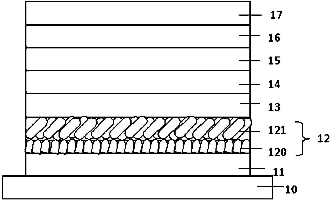
[0022] Such as figure 1 As shown, the organic electroluminescent device in this embodiment includes a substrate 10, a first electrode 11, a hole injection layer 12, a hole transport layer 13, an organic light emitting layer 14, an electron transport layer 15, and an electron injection layer stacked in sequence. 16 and the second electrode 17, the hole injection layer 12 is formed by superimposing the first inorganic nanopillar film 120 and the second inorganic nanopillar film 121, wherein the inclination angle of the inorganic nanopillars of the inorganic nanopillar film 120 is smaller than that of the inorganic nanopillar film 120. The inclination angle of the inorganic nanopillars of the nanopillar film 121 is the angle between the axial direction of the inorganic nanopillars and the normal direction of the substrate 10.

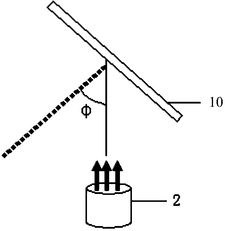
[0023] The inclination angle of the inorganic nanopillars is generally realized by evaporation, that is, during evaporation, the axial direc...

Example Embodiment

[0033] Example 2

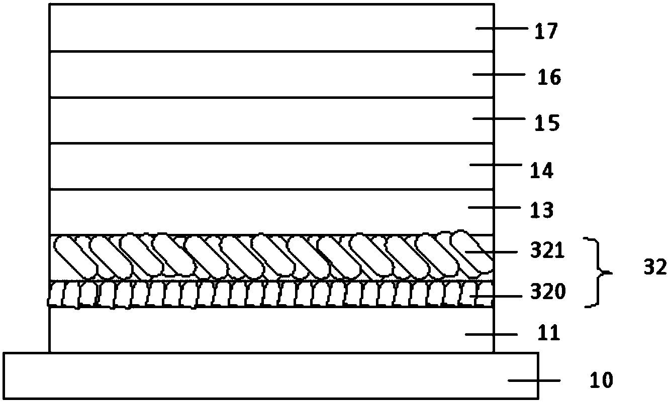
[0034] Such as image 3 As shown, the structure of the organic electroluminescence device in this embodiment is the same as the structure of the organic electroluminescence device in embodiment 1, except that the first inorganic nanopillar film 120 constituting the hole injection layer 12 The growth angle of the inorganic nanopillars of the second layer of inorganic nanopillar film 121 ranges from 10 to 30°, and the growth angle of the inorganic nanopillars of the second layer of inorganic nanopillar film 121 ranges from -45 to -85°

Example Embodiment

[0035] Example 3

[0036] The structure of the organic electroluminescence device in this embodiment is the same as the structure of the organic electroluminescence device in embodiment 1, except that the first inorganic nanopillar film 120 that constitutes the hole injection layer 12 has an inorganic nanometer structure. The growth angle of the pillars ranges from -10° to -30°, and the growth angle of the inorganic nanopillars of the second inorganic nano pillar film 121 ranges from 45° to 85°.


PUM


Abstract

The invention discloses an organic electroluminescence device. The organic electroluminescence device comprises a substrate, a first electrode, a hole injection layer, a hole transmission layer, an organic light emitting layer, an electron transmission layer, an electron injection layer and a second electrode, wherein the substrate, the first electrode, the hole injection layer, the hole transmission layer, the organic light emitting layer, the electron transmission layer, the electron injection layer and the second electrode are sequentially stacked. The hole injection layer comprises two thin inorganic nano-rod films which are vertically stacked. The inclination angles of inorganic nano-rods of the thin inorganic nano-rod film at the side close to the substrate are smaller than the inclination angles of inorganic nano-rods of the thin inorganic nano-rod film at the side far away from the substrate. The thin inorganic nano-rod film with the smaller inclination angles is beneficial to the increase of the effective contact area between the hole injection layer and an adjacent electrode layer, the barrier height, from an anode to the hole injection layer, of a hole is effectively reduced, and the starting voltage and the working voltage are reduced. The thin inorganic nano-rod film with the larger inclination angles can effectively adjust the balance of electrons and the hole, the gap scattering property of the inclined nano-rods is used, so that on the premise that power efficiency is not sacrificed, the luminous efficiency is improved. The invention further discloses a preparing method of the organic electroluminescence device.

Description

technical field [0001] The invention belongs to the technical field of organic electroluminescence display, and in particular relates to an organic electroluminescence device and a preparation method thereof. Background technique [0002] As a new type of semiconductor display technology, organic electroluminescent technology has recently made great achievements in the fields of small and medium-sized mobile devices and large-sized displays. The light-emitting mechanism of organic light-emitting diode (OLED) is that under the action of an external electric field, electrons and holes are injected from the cathode and anode to the organic functional film, respectively, and the injected electrons and holes are transported from the electrons respectively. Layer and hole transport layer migrate to the light-emitting layer, recombine in the light-emitting layer to form excitons, and excitons radiatively transition to generate photons to complete the light-emitting process. [000...

Claims


Application Information

Patent Timeline
IPC IPC(8): H01L51/50H01L51/56
CPCH10K71/164H10K50/17H10K71/00
Inventor 朱儒晖任海魏锋赵芳
Owner SICHUAN CCO DISPLAY TECH
Why Eureka
Try Eureka