Novel LTCC double-layer single-feed circular polarization micro-strip patch array antenna

A microstrip patch and array antenna technology, which is applied to antenna unit combinations, antennas, slot antennas and other directions with different polarization directions, can solve the problem of high requirements on the dimensional accuracy of the patch cut angle, increasing the complexity of the antenna structure, and disadvantageous antennas. Miniaturization and other issues, to achieve the effect of more size, simple structure and easy processing

Inactive Publication Date: 2014-06-18
UNIV OF ELECTRONIC SCI & TECH OF CHINA
2 Cites 26 Cited by

AI-Extracted Technical Summary

Problems solved by technology

At present, the common methods of widening the microstrip patch antenna include increasing the thickness of the substrate, adopting a multi-layer structure, and adding impedance matching, etc., but these are not only not conducive to the miniaturization of the antenna, but also make the antenna structure more complicated.
In addition, in realizing the circular polarization of the microstrip patch antenna, there are currently common methods of using m...

Method used

[0031] Upper LTCC substrate 1: the substrate adopts 10 thicknesses of 0.1mm, and a dielectric constant of 5.9 LTCC cast film lamination, the substrate transverse dimension is 74.2mm, and the longitudinal dimension is 76.3mm. The upper surface of the substrate is printed with 4X4 units of radiating metal patches of the same size with silver paste to form an upper radiating metal patch antenna array. The radiating metal patch is 8mm away from the left and right sides of the substrate, and 9.4mm away from the upper and lower sides. The radiating metal p...

Abstract

The invention aims to provide a double-layer single-feed circular polarization micro-strip patch array antenna based on the LTCC technology. The double-layer single-feed circular polarization micro-strip patch array antenna comprises an upper LTCC substrate, a lower LTCC substrate, a feed network, an upper radiation metal patch antenna array, a lower radiation metal patch antenna array, a metal probe, a feed port and a grounded metal layer, wherein the lower radiation metal patch antenna array and the feed network are arranged on the upper surface of the lower LTCC substrate, and the upper radiation metal patch antenna array is located on the upper surface of the upper LTCC substrate; the upper radiation metal patch antenna array and the lower radiation metal patch antenna array have the same shape and size, each antenna array is composed of four sub-arrays, each sub-array is composed of four radiation metal patches, each radiation metal patch is in a chamfered square shape, and rectangular gaps are formed in a set of opposite edges of each radiation metal patch. According to the double-layer single-feed circular polarization micro-strip patch array antenna, better consideration is given to performance requirements for the low profile, circular polarization and high gain of the micro-strip patch array antenna, and meanwhile the frequency band width of the antenna is increased greatly.

Application Domain

Technology Topic

Image

  • Novel LTCC double-layer single-feed circular polarization micro-strip patch array antenna
  • Novel LTCC double-layer single-feed circular polarization micro-strip patch array antenna
  • Novel LTCC double-layer single-feed circular polarization micro-strip patch array antenna

Examples

  • Experimental program(1)

Example Embodiment

[0028] The present invention will be further described in detail below with reference to the accompanying drawings and embodiments, but the implementation of the present invention is not limited thereto.
[0029] The center frequency of the microstrip patch array antenna provided in this embodiment is 10 GHz, such as Image 6 As shown, the present invention can achieve a microstrip patch array antenna with an impedance bandwidth of 1.5 GHz and a maximum gain exceeding 16.7 dB within a cross-sectional thickness of 2 mm, and the axial ratio of the antenna can be less than 1.5 dB.
[0030] The LTCC double-layer single-fed circularly polarized microstrip patch array antenna provided in this embodiment includes:
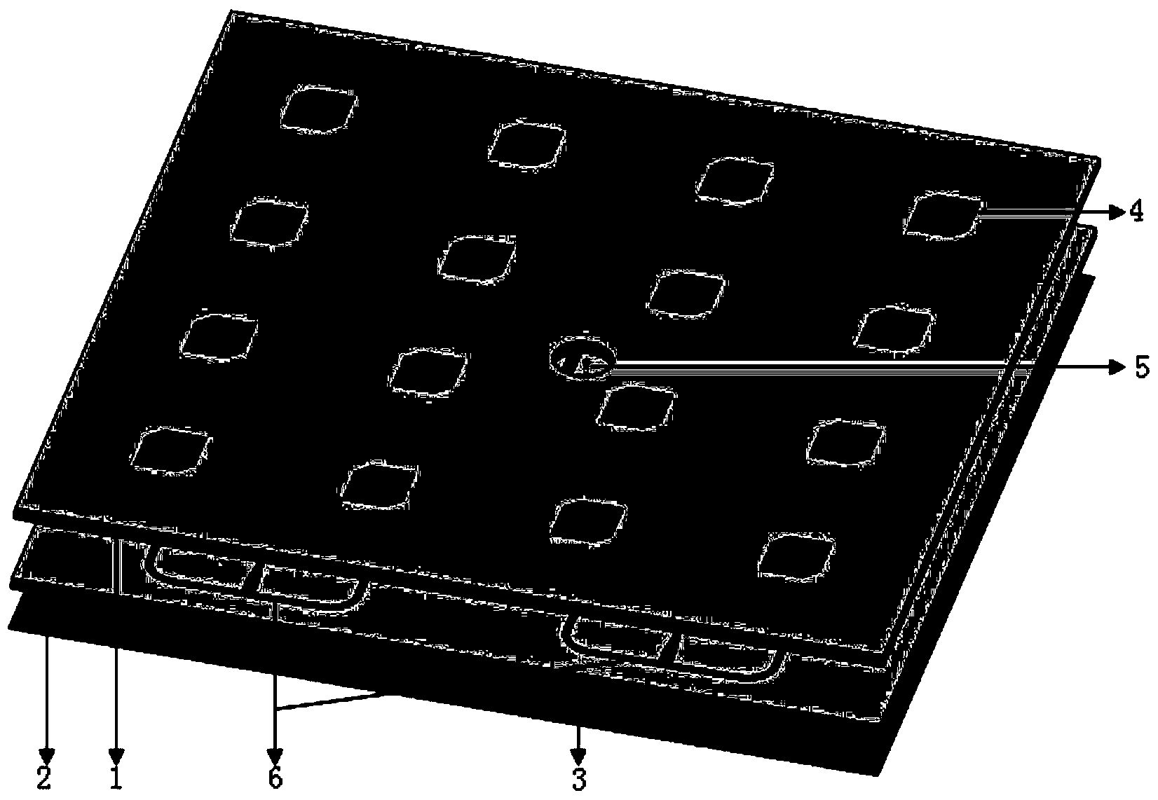
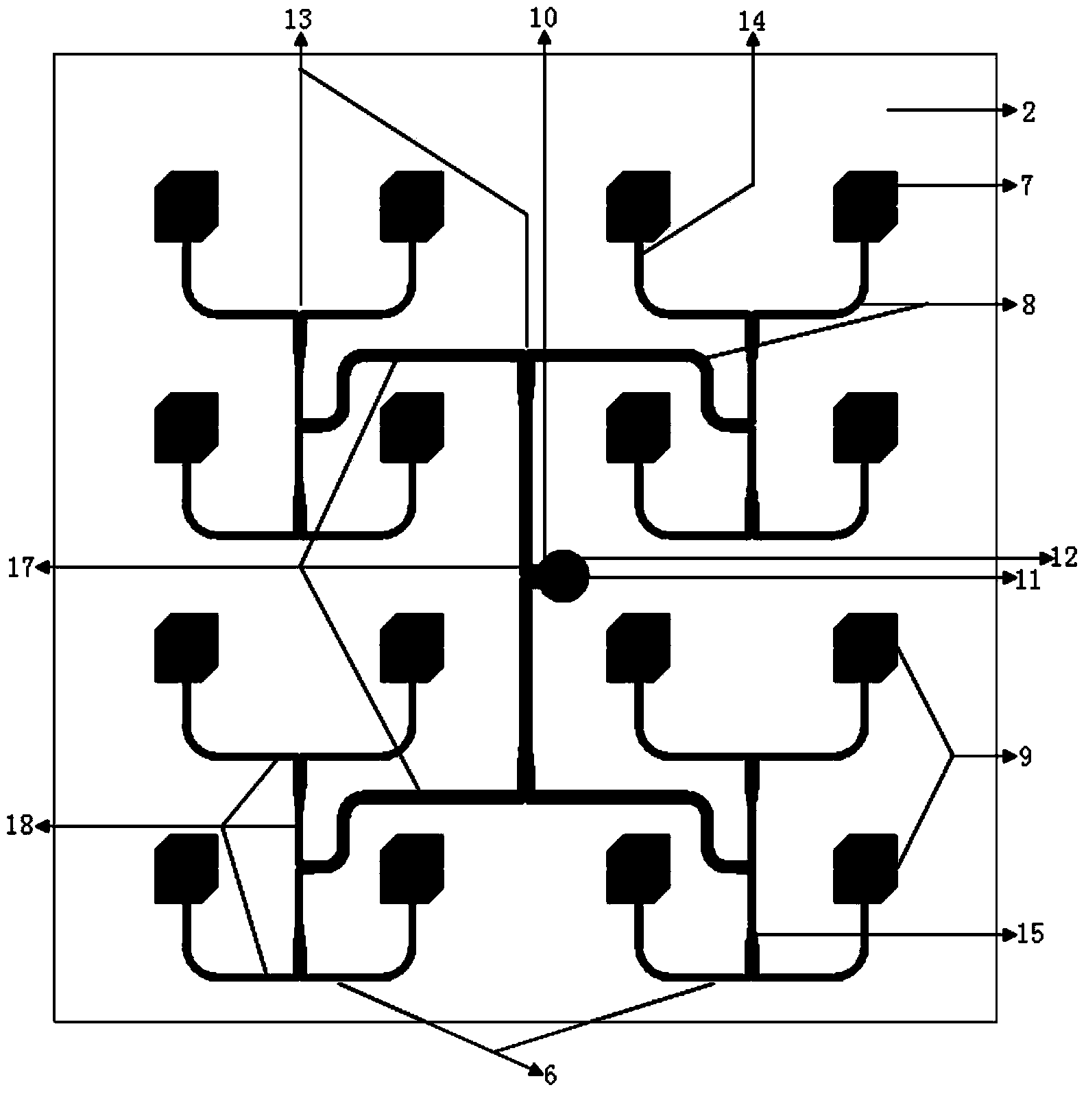
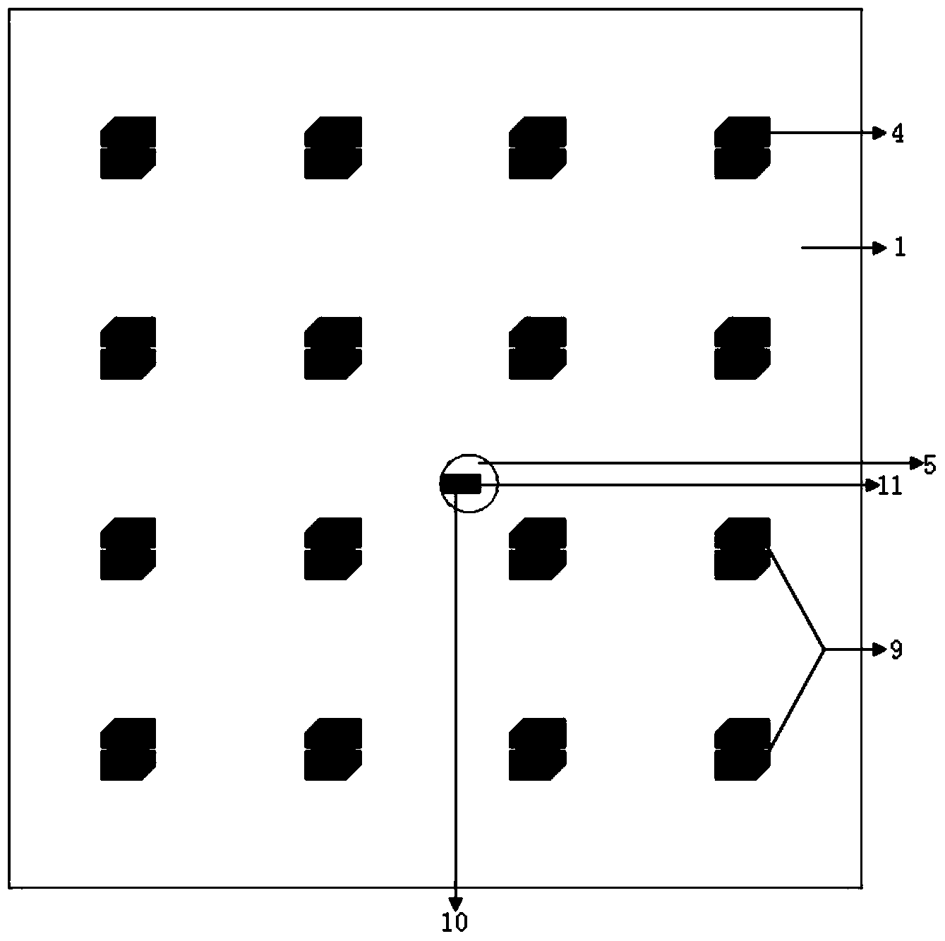
[0031] Upper LTCC substrate 1: This substrate is laminated with 10 LTCC cast films with a thickness of 0.1mm and a dielectric constant of 5.9. The lateral dimension of the substrate is 74.2mm and the longitudinal dimension is 76.3mm. The upper surface of the substrate is made of silver paste printed with 4X4 units of the same size radiating metal patch to form the upper radiating metal patch antenna array. The radiating metal patch is 8mm from the left and right sides of the substrate and 9.4mm from the upper and lower sides. The radiating metal patch The horizontal spacing between them is 17.8mm, and the longitudinal spacing is 17.4mm. Cut corners on the opposite corners of the radiating metal patch to achieve circular polarization. The cut corners are isosceles right-angled triangles with a side length of 1.2 mm, and a rectangular gap with a length of 0.6 mm and a width of 0.2 mm is opened on the opposite side. A circular window 5 with a radius of 2.5 mm is opened near the center of the substrate to expose the metal probe 11 and the 1/4 wavelength conversion section 10 to facilitate welding.
[0032] Lower LTCC substrate 2: This substrate is made by laminating 10 LTCC cast films with a thickness of 0.1 mm and a dielectric constant of 5.9. The size of the substrate is exactly the same as that of the upper substrate 1. The upper surface of the substrate is printed with 4X4 units of the same size radiating metal patch and feeder network 6 with silver paste. The structure and size of the lower radiating metal patch antenna array 7 are exactly the same as the upper radiating metal patch antenna array 4, and its position on the lower substrate is exactly the same as the position of the upper radiating metal patch antenna array 4 on the upper substrate. The length of the strip lines 14 and 10 is 1/4 times of the propagation wavelength in the medium. The sweep elbow 8 connected to the 1/4 wavelength conversion section 14 is a 1/4 ring with a radius of 2.7mm, which is not connected to 1/ The swept elbows 8 connected to the 4 wavelength conversion sections 14 are all quarter rings with a radius of 2 mm. The 1/4 wavelength conversion section 14 is located at the geometric center of the bottom edge of the lower radiating metal patch 7 before the corner is not cut. When other strip transmission lines of different sizes are connected, the geometric centers of the connecting sides overlap, and the strip transmission lines 17 are adjacent to each other. The distance between the metal radiation patch and the strip line or the radiation patch and the radiation patch is the same. The chamfered corners 13 at the T-joint are all isosceles triangles. A through hole with a radius of 0.65mm is opened near the middle of the substrate. The center of the through hole is the same distance from the upper and lower sides of the 1/4 wavelength conversion section 10, and the distance from the right is 0.95mm. The through hole is for inserting the metal probe 11. The width of the feeding network 6 is optimized to ensure that the impedance of the 1/4 wavelength conversion section 10 is 50 ohms, the impedance of the strip line 17 is 75 ohms, and the impedance of the 1/4 wavelength conversion section 14 is 100 ohms.
[0033] Ground metal layer 3: The ground metal layer 3 is located on the lower surface of the lower LTCC substrate 2 and has a circular hole 16 with a radius of 2 mm near the middle. The geometric centers of the circular hole 16, the metal probe 11 and the circular window 5 on the upper LTCC substrate 1 are on the same Z axis.

PUM

no PUM

Description & Claims & Application Information

We can also present the details of the Description, Claims and Application information to help users get a comprehensive understanding of the technical details of the patent, such as background art, summary of invention, brief description of drawings, description of embodiments, and other original content. On the other hand, users can also determine the specific scope of protection of the technology through the list of claims; as well as understand the changes in the life cycle of the technology with the presentation of the patent timeline. Login to view more.

Similar technology patents

Classification and recommendation of technical efficacy words

  • Simple structure
  • Easy to process

Microlithographic projection exposure apparatus

InactiveUS20050068499A1Simple structureReliable and low-maintenance operationProjectorsPhotomechanical exposure apparatusCamera lensPhysics
Owner:CARL ZEISS SMT GMBH

Graphite Nanocomposites

Owner:EXXONMOBIL CHEM PAT INC
Why Eureka
Try Eureka