Method for achieving atomic force microscope (AFM) nano deposition by applying current

An atomic force microscope and current-applying technology, applied in the direction of nanotechnology, nanotechnology, nanostructure manufacturing, etc., can solve problems such as unguaranteed, uneven deposition points, and no fixation, etc., to achieve flexible control, good repeatability, and high precision Effect

Inactive Publication Date: 2014-06-25
SHENYANG INST OF AUTOMATION - CHINESE ACAD OF SCI
View PDF2 Cites 3 Cited by
  • Summary
  • Abstract
  • Description
  • Claims
  • Application Information

AI Technical Summary

Problems solved by technology

[0003] 1. The nanomaterials are naturally lapped on the electrode, and no good fixation is formed.
[0004] 2. There is a large contact resistance between nanomaterials and electrodes, which affects the performance of the device in terms of conductivity and anti-interference
At present, AFM nano-deposition mostly adopts the method of applying voltage pulses. The repeatability and controllability of this processing method are not ideal, and the success of each deposition process cannot be guaranteed, and the deposition point of the process is not uniform, and the height of the deposition point is several nanometers. and vary between hundreds of nanometers
Moreover, the current method of processing nanowires is to process a series of nanodots, and the nanodots are arranged into lines, which requires multiple processing and the nanowires are not smooth.

Method used


Image

  • Method for achieving atomic force microscope (AFM) nano deposition by applying current
  • Method for achieving atomic force microscope (AFM) nano deposition by applying current
  • Method for achieving atomic force microscope (AFM) nano deposition by applying current

Examples


Embodiment Construction

[0024] The present invention will be further described in detail below in conjunction with the accompanying drawings and embodiments.

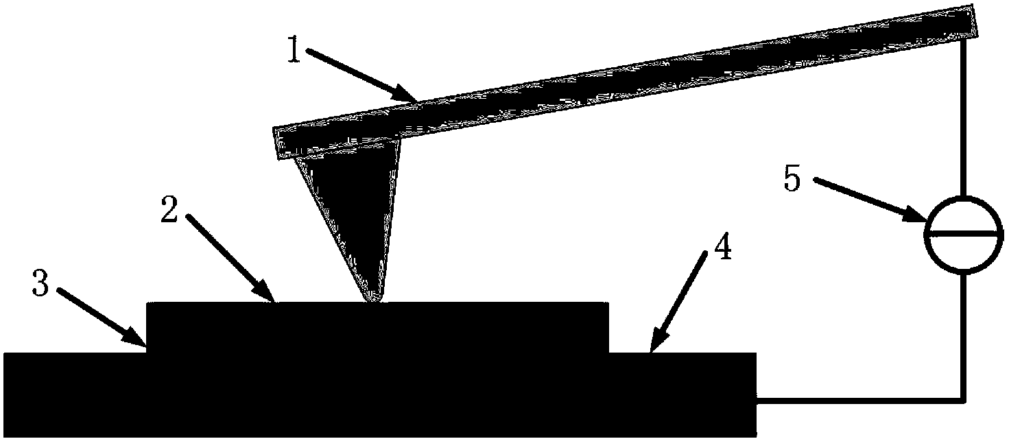
[0025] figure 1 It is a schematic diagram of the working state of the present invention. Among them, 1 is the AFM conductive probe, 2 is the substrate, 3 is the conductive glue, 4 is the metal sample stage, and 5 is the programmable current source.

[0026] The processing method is:

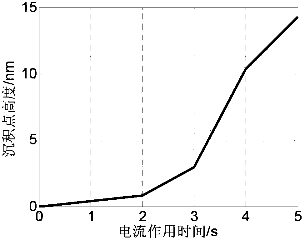
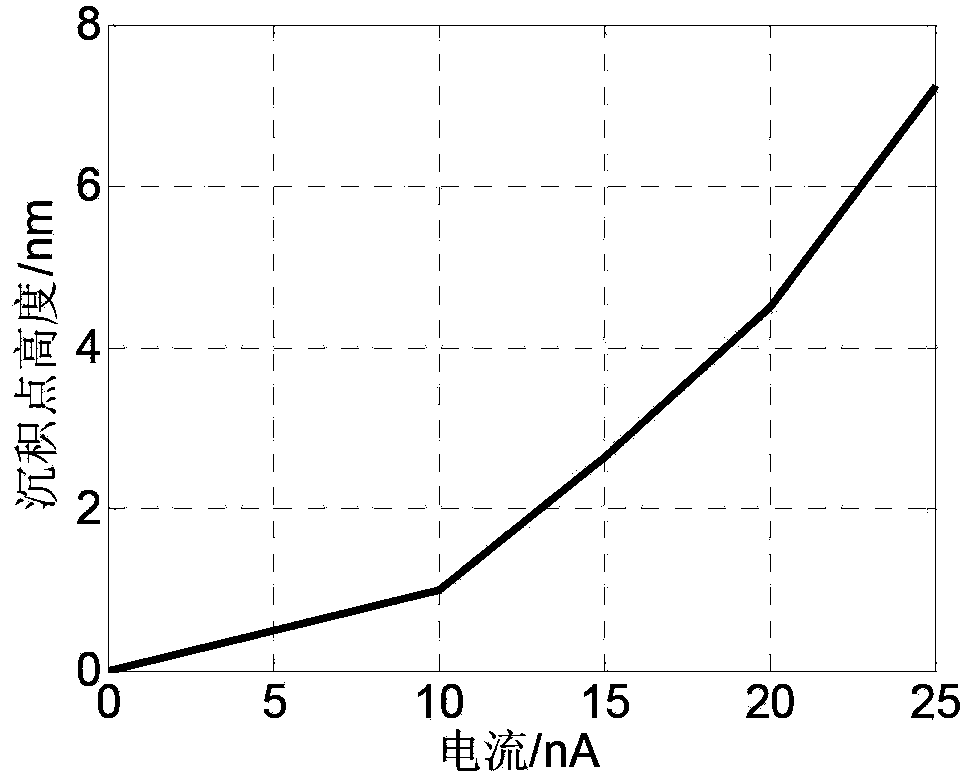
[0027] 1) Determine the parameters of the current applied during machining. The height of the deposition point is related to the size of the current and the time of the current. Figure 2 is the relationship curve of deposition point height, current magnitude and current action time calculated from the results of a large number of AFM nano-deposition experiments carried out in advance. This line can be used as the basis for current parameters when processing deposition points of different sizes. According to the height of the desired processing deposition poin...


PUM


Abstract

The invention discloses a method for achieving atomic force microscope (AFM) nano deposition by applying a current. According to the method, by means of application of the certain current onto an AFM pinpoint and substrate and control of the magnitude of the current, atoms on an AFM conducting probe are deposited on the substrate to form a conductor deposition point, and the conductor deposition point can be used for processing a nano lattice structure and welding nano materials in a nano device. By means of the method for achieving AFM nano deposition by applying the current, the deposition point with good repeatability and high precision can be processed, and meanwhile, the size of the deposition point can be flexibly controlled; the method can be used for processing nanowires.

Description

technical field [0001] The invention relates to the field of nano-processing, in particular to a processing method for applying current between the probe of an atomic force microscope and a substrate, so that the material on the surface of the probe tip moves to the substrate and accumulates into nano-dots. Background technique [0002] Nano-devices are electronic devices composed of nano-materials, such as various gas sensors, biosensors, field-effect transistors, and so on. Nano-devices have excellent properties, such as the Coulomb blocking effect and so on. However, nano-devices have not been widely used at present, because there are still some problems in the processing and manufacturing of nano-devices, one of which is the electrical connection problem of nano-devices. Nano-devices are formed by assembling nano-materials and metal electrodes. The electrical connection problems after assembly are as follows: [0003] 1. The nanomaterials are naturally overlapped on th...

Claims


Application Information

Patent Timeline
Patent Type & Authority Applications(China)
IPC IPC(8): B82B3/00B82Y40/00
Inventor 焦念东刘增磊刘连庆
Owner SHENYANG INST OF AUTOMATION - CHINESE ACAD OF SCI
Why Eureka
Try Eureka