A zinc sulfide thin film AC electroluminescent device containing doped quantum dots and its preparation method
An alternating current and electroluminescence technology, applied in electrical components, semiconductor devices, circuits, etc., can solve the problems of high vacuum, complex process, inability to achieve wide application, etc., and achieve the effect of improving excitation efficiency, improving luminous efficiency, and simple process
- Summary
- Abstract
- Description
- Claims
- Application Information
AI Technical Summary
Problems solved by technology
Method used
Image

Examples
Embodiment 1
[0023] The preparation of this device includes the following steps:
[0024] (1) Preparation of the first insulating layer
[0025] Firstly, ultrasonically clean and dry the ITO conductive glass layer 5 . Plating Ta on ITO electrodes by electron beam thermal evaporation 2 o 5 The insulating layer is the first insulating layer 4 .
[0026] (2) Preparation of zinc sulfide sol-gel
[0027] Zinc acetate (Zn(CH 3 COO) 2 2H 2 O) solution and ethylenediamine (En) were stirred evenly in a beaker, and a small amount of hydrochloric acid was added. Thereafter, thioacetamide was added with stirring. Finally, a small amount of hydrochloric acid was added to obtain ZnS sol-gel.
[0028] (3) Preparation of doped semiconductor quantum dots CdS:Mn / ZnS
[0029] CdS:Mn / ZnS was synthesized by Growth-doping method. Firstly, the precursors of Cd, CdO, Oleic acid, and ODE were stirred and degassed for 15 minutes in an Ar gas environment in a three-necked flask, and the precursor of S w...
Embodiment 2
[0039] This embodiment is basically the same as Embodiment 1, except that the glass sheet after film formation is annealed at 150° C. in argon, and the film thickness is controlled at 500 nm.
Embodiment 3
[0041] This embodiment is basically the same as Embodiment 1, except that the glass sheet after film formation is annealed at 200° C. in argon, and the film thickness is controlled at 1000 nm.
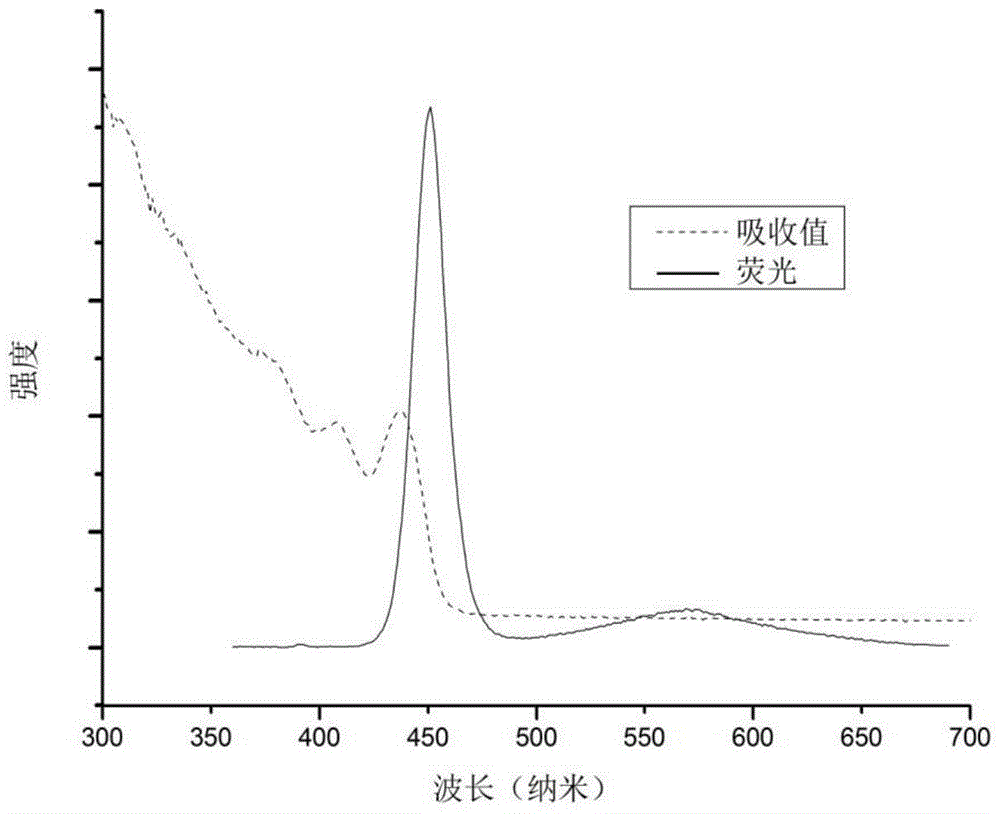
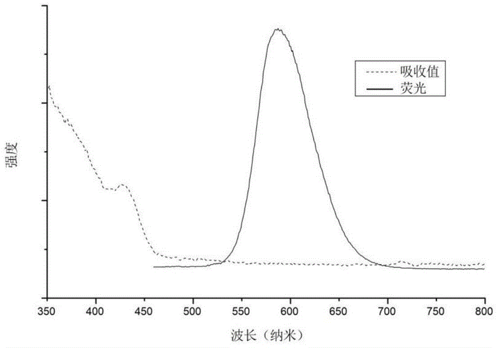
[0042] Get the CdS of embodiment 1 gained and CdS:Mn / ZnS semiconductor quantum dot nanometer material carries out absorption and fluorescence spectrum test and obtains figure 1 and figure 2 ,from figure 1 It can be seen that the absorption peak and fluorescence emission peak of CdS are obvious, indicating that the CdS core has been formed and can be used to further synthesize CdS:Mn / ZnS semiconductor quantum dots. figure 2 , it can be seen that the absorption and fluorescence peaks of CdS:Mn / ZnS semiconductor quantum dots are obvious, indicating that CdS:Mn / ZnS semiconductor quantum dots have been formed and can be used to prepare thin films.
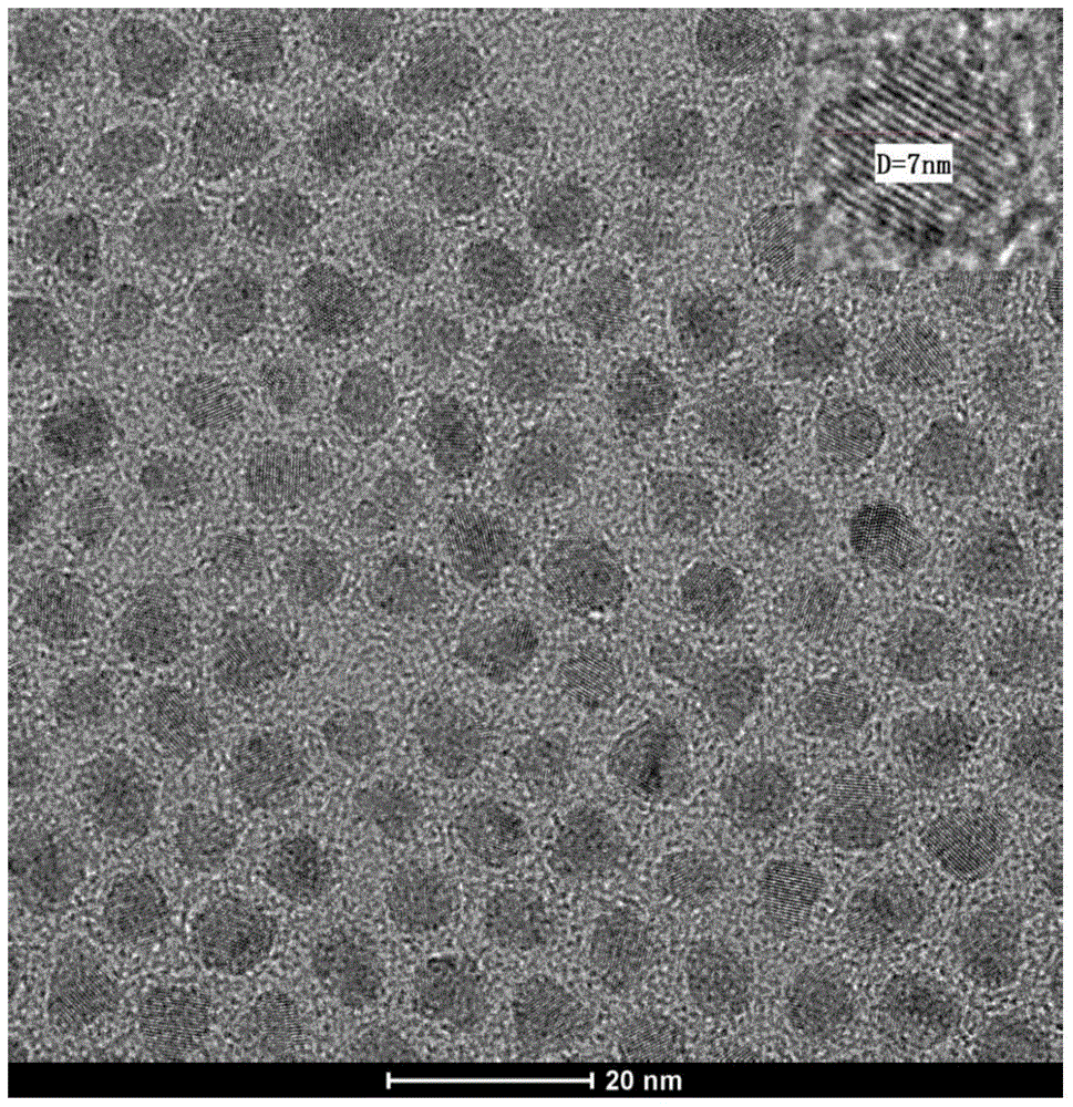
[0043] Get the CdS of embodiment 1 gained: Mn / ZnS semiconductor quantum dot nanometer material carries out transmission electron microscope...
PUM
| Property | Measurement | Unit |
|---|---|---|
| thickness | aaaaa | aaaaa |
| diameter | aaaaa | aaaaa |
Abstract
Description
Claims
Application Information
 - R&D
- Intellectual Property
- Life Sciences
- Materials
- Tech Scout
- Unparalleled Data Quality
- Higher Quality Content
- 60% Fewer Hallucinations
Browse by: Latest US Patents, China's latest patents, Technical Efficacy Thesaurus, Application Domain, Technology Topic, Popular Technical Reports.
© 2025 PatSnap. All rights reserved.Legal|Privacy policy|Modern Slavery Act Transparency Statement|Sitemap|About US| Contact US: help@patsnap.com