Semiconductor laser heat sink with graphene layer and manufacturing method thereof

A graphene layer and laser technology, applied in the direction of semiconductor lasers, structural details of semiconductor lasers, lasers, etc., can solve problems such as unfavorable heat dissipation of semiconductor lasers, and achieve the goal of ensuring photoelectric performance and reliability, excellent electrical conductivity, and improving heat dissipation Effect

Active Publication Date: 2014-06-25
BEIJING PEONY ELECTRONICS GROUP CORP
View PDF6 Cites 23 Cited by
  • Summary
  • Abstract
  • Description
  • Claims
  • Application Information

AI Technical Summary

Problems solved by technology

[0005] The technical problem to be solved by the present invention is to provide a semiconductor laser heat sink with a graphene layer and its manufacturin

Method used


Image

  • Semiconductor laser heat sink with graphene layer and manufacturing method thereof

Examples


Embodiment Construction

[0027] The principles and features of the present invention are described below in conjunction with the accompanying drawings, and the examples given are only used to explain the present invention, and are not intended to limit the scope of the present invention.

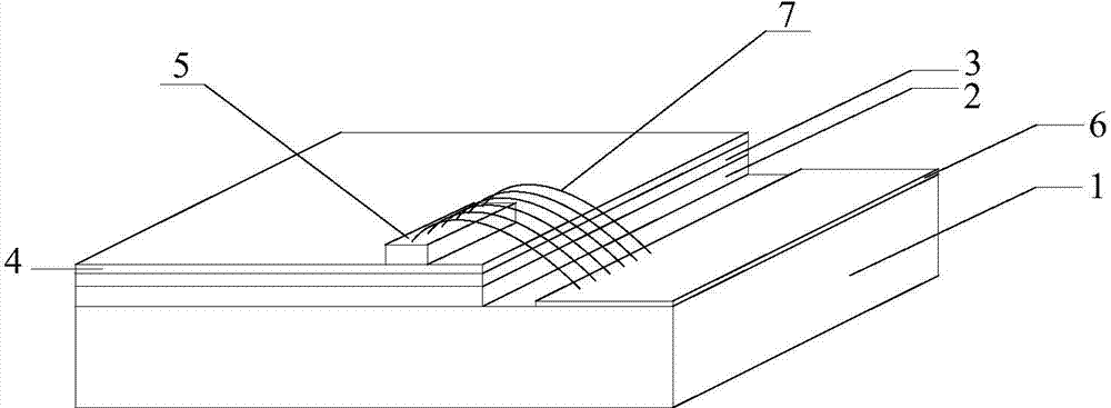
[0028] like figure 1 As shown, the present embodiment provides a heat sink of a semiconductor laser, including a base material layer 1, an oxygen-free copper layer 2 and a graphene layer 3 deposited sequentially from bottom to top, and the material used in the base material layer 1 is Any one of aluminum nitride ceramics, alumina ceramics, zirconia ceramics, silicon nitride ceramics, silicon carbide or boron nitride.

[0029] In this embodiment, the graphene layer 3 is plated with a solder layer 4 , and the solder layer 4 is used for welding the semiconductor laser 5 . The base material layer 1 is also plated with a gold layer 6 insulated from the oxygen-free copper layer 2, and a gold wire 7 is welded on the gold ...


PUM


Abstract

The invention relates to a semiconductor laser heat sink with a graphene layer. The semiconductor laser heat sink with the graphene layer comprises a base material layer, an oxygen-free copper layer and the graphene layer which sequentially deposit from bottom to top, wherein the base material layer is made of any one of aluminum nitride ceramics, aluminum oxide ceramics, zirconia ceramics, silicon nitride ceramics, silicon carbide and boron nitride. The invention further relates to a method for manufacturing the semiconductor laser heat sink. The graphene layer is adopted as heat dissipation materials of the heat sink, the physical property of high heat conductivity of graphene is fully used, the heat generated when a semiconductor laser works is conducted out and dissipated, under the condition of not increasing the weight and the size of the semiconductor laser, the heat dissipation capacity of the semiconductor laser is largely improved, the temperature of the semiconductor laser in the working process is lowered, the photoelectric property and reliability of the semiconductor laser are guaranteed, and the service life of the semiconductor laser is prolonged.

Description

technical field [0001] The invention relates to the technical field of semiconductor device packaging, in particular to a heat sink with a graphene layer used for packaging high-power semiconductor lasers and a manufacturing method thereof. Background technique [0002] High-power semiconductor lasers have the advantages of small size, high electro-optical conversion efficiency, wide band coverage, and easy integration. At present, it has been widely used in laser ranging, laser communication, material processing, mechanical processing and medical and health fields. However, with the continuous improvement of the output power of semiconductor lasers, a large part of the electrical power is converted into thermal power. The optical characteristics, output power and reliability of semiconductor lasers are closely related to the operating temperature of the device. Therefore, heat dissipation has become a key factor that directly affects the performance of semiconductor laser...

Claims


Application Information

Patent Timeline
IPC IPC(8): H01S5/024H01S5/02
Inventor 李刚张松崔碧峰徐旭红赵瑞计伟
Owner BEIJING PEONY ELECTRONICS GROUP CORP
Why Eureka
Try Eureka