Inversion organic thin film solar cell decorated by polar solvent and preparing method thereof

A solar cell and polar solvent technology, applied in circuits, photovoltaic power generation, electrical components, etc., can solve the problems of improving the conductivity of PEDOT:PSS thin films, restricting the carrier hole transport rate, and hindering carrier transport, etc. Achieve the effect of improving carrier transport efficiency, increasing carrier transport efficiency, and reducing recombination probability

Inactive Publication Date: 2014-07-02
UNIV OF ELECTRONICS SCI & TECH OF CHINA
View PDF4 Cites 8 Cited by
  • Summary
  • Abstract
  • Description
  • Claims
  • Application Information

AI Technical Summary

Problems solved by technology

[0004] At present, the main reasons for limiting the application of PEDOT:PSS anode buffer layer are: firstly, after PEDOT:PSS is prepared as an anode buffer layer, the hydrophilic and non-conductive PSS groups will gather on the surface of the film, thereby hindering the flow of carriers. Second, the main PEDOT group that transports holes cannot be effectively separated from the hydrophilic and non-conductive PSS group after film formation, thus restricting the transport rate of carrier holes in the anode buffer layer
The traditional solution is to add a certain amount of additives to the PEDOT:PSS solution to separate the PEDOT and PSS groups, but the additives cannot be removed so that it becomes a non-conductive trap center, which restricts the conductivity of the PEDOT:PSS film. Further improve

Method used


Image

  • Inversion organic thin film solar cell decorated by polar solvent and preparing method thereof
  • Inversion organic thin film solar cell decorated by polar solvent and preparing method thereof
  • Inversion organic thin film solar cell decorated by polar solvent and preparing method thereof

Examples


Embodiment 1

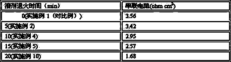
[0035] Embodiment 1 (comparative example):

[0036] Clean the substrate composed of transparent substrate and transparent conductive cathode ITO with surface roughness less than 1 nm, and then dry it with nitrogen; spin-coat ZnO (5000 rpm, 40 s, 15 nm) on the surface of transparent conductive cathode ITO, and The formed film was baked (200°C, 60 min) to obtain a cathode buffer layer; a photoactive layer of P3HT:PCBM (1:20, 20 mg / ml) was prepared on the cathode buffer layer by spin coating (1000 rpm, 25 s , 220 nm), and baked (140°C, 5 min); spin-coat PEDOT:PSS solution (3000 rpm, 60 s, 30 nm) on the surface of the photoactive layer to prepare the anode buffer layer; Annealing was performed by heating annealing (150°C, 5 min); metal anode Ag (100 nm) was vapor-deposited on the anode solvent buffer layer. Under standard test conditions: AM 1.5, 100 mW / cm 2 , the open circuit voltage of the device was measured (V OC )=0.54 V, short-circuit current (J SC )=8.6 mA / cm 2 , fill ...

Embodiment 2

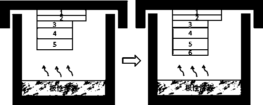
[0038]Clean the substrate composed of transparent substrate and transparent conductive cathode ITO with surface roughness less than 1 nm, and then dry it with nitrogen; spin-coat ZnO (5000 rpm, 40 s, 15 nm) on the surface of transparent conductive cathode ITO, and The formed film was baked (200°C, 60 min) to obtain a cathode buffer layer; a photoactive layer of P3HT:PCBM (1:20, 20 mg / ml) was prepared on the cathode buffer layer by spin coating (1000 rpm, 25 s , 220 nm), and baked (140°C, 5 min); spin-coat PEDOT:PSS solution (3000 rpm, 60 s, 30 nm) on the surface of the photoactive layer to prepare the anode buffer layer; on the surface of the anode buffer layer, use The polar solvent buffer layer was prepared by solvent evaporation annealing method (95 % dimethyl sulfoxide, 5 % ethanol, 5 nm, 5 min); the substrate was annealed by heating and annealing on a constant temperature hot stage (150 ° C, 5 min); Metal anode Ag (100 nm) was evaporated on the polar solvent buffer layer....

Embodiment 3

[0040] Clean the substrate composed of transparent substrate and transparent conductive cathode ITO with surface roughness less than 1 nm, and then dry it with nitrogen; spin-coat ZnO (5000 rpm, 40 s, 15 nm) on the surface of transparent conductive cathode ITO, and The formed film was baked (200°C, 60 min) to obtain a cathode buffer layer; a P3HT:PCBM (1:20, 20 mg / ml) photoactive layer (1000 rpm, 25 s, 220 nm), and baked (140°C, 5 min); spin-coat PEDOT:PSS solution on the surface of the photoactive layer to prepare an anode buffer layer (3000 rpm, 60 s, 28 nm); on the anode buffer layer The surface was prepared with a polar solvent buffer layer (96 % dimethyl sulfoxide, 4 % ethanol, 5 nm, 15 min) by solvent evaporation annealing method; the substrate was annealed by heating and annealing on a constant temperature hot stage (150 ° C, 5 min); Metal anode Ag (100 nm) was evaporated on the polar solvent buffer layer. Under standard test conditions: AM 1.5, 100 mW / cm 2 , the open...


PUM


Abstract

The invention discloses an inversion organic thin film solar cell decorated by a polar solvent and a preparing method of the inversion organic thin film solar cell and relates to the field of organic polymer photovoltaic devices or organic semiconductor thin film solar cells. An inversion structure is adopted in the solar cell. The solar cell comprises a substrate, a transparent conductive cathode ITO, a cathode buffer layer, a light active layer, an anode buffer layer, a polar solvent buffer layer and a metal anode. The polar solvent buffer layer is added to the portion between the anode buffer layer and the light active layer of the solar cell, the conductivity of the anode buffer layer can be effectively improved, the series resistance of devices is reduced, the carrier transporting efficiency is improved, and the photoelectric conversion efficiency of the solar cell is finally improved.

Description

technical field [0001] The invention belongs to the field of organic polymer photovoltaic devices or organic semiconductor thin-film solar cells, and in particular relates to polar solvent-modified inverted organic thin-film solar cells and a preparation method thereof. Background technique [0002] With the explosive growth of the global energy demand, the energy problem has become the primary problem faced by the economic development of all countries. Because solar energy is clean, widely distributed, and inexhaustible, research on photovoltaic power generation to solve energy problems has become the focus and focus of research in the field of renewable energy. Currently, active layer materials can be classified into inorganic semiconductor materials and organic semiconductor materials according to the different properties of materials that make up the photoactive layer of a solar cell. Compared with inorganic semiconductor materials, organic semiconductor materials n...

Claims


Application Information

Patent Timeline
Patent Type & Authority Applications(China)
IPC IPC(8): H01L51/42H01L51/44H01L51/46H01L51/48
CPCY02E10/549H10K71/164H10K30/20H10K30/81Y02P70/50
Inventor 于军胜郑毅帆李曙光钟建
Owner UNIV OF ELECTRONICS SCI & TECH OF CHINA
Why Eureka
Try Eureka