Multi-frequency response TeraHertz wave modulator

A terahertz wave and modulator technology, which is applied in the field of terahertz wave modulators, can solve the problems of complex preparation process, inability to realize modulation, and low modulation depth, etc., achieve short preparation process, reduce preparation cost, and reduce use cost Effect

Inactive Publication Date: 2014-08-13
SOUTHEAST UNIV
View PDF5 Cites 23 Cited by
  • Summary
  • Abstract
  • Description
  • Claims
  • Application Information

AI Technical Summary

Problems solved by technology

Chen Heming of Nanjing University of Posts and Telecommunications proposed that the modulation of dual-wavelength terahertz waves can be realized based on nonlinear photonic crystals [2][3], but the preparation process of this terahertz wave modulator is complicated and difficult to realize in practice
H.T.Chen engraved the metal microstrip structure on the semiconductor substrate by micromachining technology, and realized the control of the terahertz wave by changing the capacitance [4]. The substrate used was a silicon-sapphire wafer, and the conductivity of silicon was greater than 100Ω. cm, using the optical pumping THz detection technology to excite the silicon surface, the central frequency of the terahertz wave can be adjusted within 20% by controlling the photogenerated carriers with external light, but the modulation depth of this method is not High, and it is impossible to simultaneously modulate several terahertz waves of different wavelengths (frequency)
[0004] see figure 1 , some researchers have proposed a terahertz modulator based on a semiconductor substrate and a metamaterial structure, but since the metamaterial structure on the semiconductor substrate of the device has only one size, it cannot flexibly and conveniently control the terahertz modulator of multiple frequencies. The wave is modulated, and the cost of its preparation is also high, which limits the wider use of this kind of terahertz modulator

Method used


Image

  • Multi-frequency response TeraHertz wave modulator
  • Multi-frequency response TeraHertz wave modulator
  • Multi-frequency response TeraHertz wave modulator

Examples


Embodiment Construction

[0024] The present invention will be further described below in conjunction with the accompanying drawings.

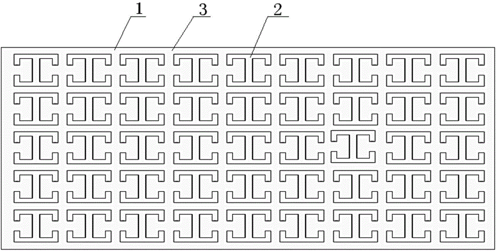
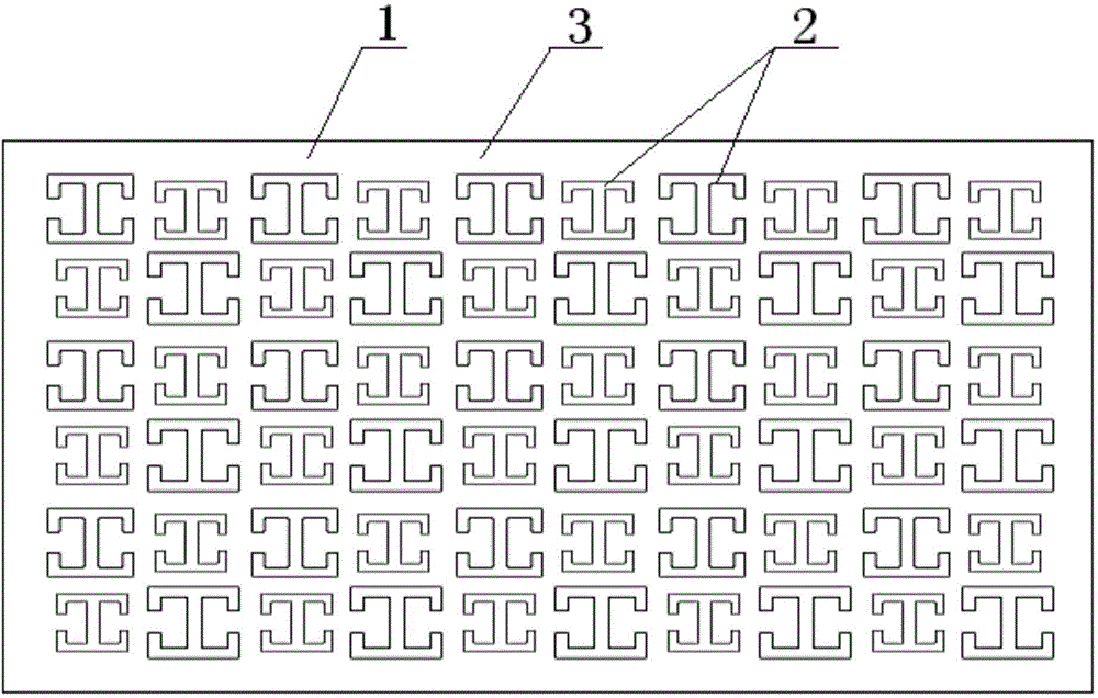
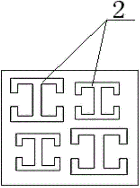
[0025] like figure 2 Shown is a multi-frequency response terahertz wave modulator, including a semiconductor substrate 1 on which terahertz waves can be projected, a metamaterial resonance unit 2 of two sizes and a metal titanium thin film layer 3, the metamaterial resonance unit 2 is arranged on the semiconductor substrate 1, and the metal titanium thin film layer 3 is arranged on the metamaterial resonance unit 2 and the semiconductor substrate 1; all metamaterial resonance units 2 of the same size are arranged on the semiconductor substrate 1 in a periodic array manner On the above, two kinds of metamaterial resonant units 2 of different sizes are arranged in a staggered manner, and there are gaps between different metamaterial resonator units 2 .

[0026] All metamaterial resonance units 2 in this case can be divided into several metamaterial resonance unit group...


PUM

PropertyMeasurementUnit
thicknessaaaaaaaaaa

Abstract

The invention discloses a multi-frequency response TeraHertz wave modulator, which comprises a semiconductor substrate capable of being transmitted by TeraHertz wave, metamaterial resonance units with more than two dimensions, and a metallic titanium film layer, wherein the metamaterial resonance units are arranged on the semiconductor substrate, the metallic titanium film layer is arranged on the metamaterial resonance units and the semiconductor substrate, all the metamaterial resonance units with the same dimension are arranged on the substrate in a periodic matrix manner, metamaterial resonance units with different dimensions are arranged in a staggered manner, and gaps exist among different metamaterial resonance units. According to the multi-frequency response TeraHertz wave modulator disclosed by the invention, a two-frequency TeraHertz wave modulator or a multi-frequency TeraHertz wave modulator is integrated on the substrate, and TeraHertz waves with two kinds and multiple kinds of frequencies are modulated according to needs, in such a way, the use cost is favorably reduced, and the multi-frequency response TeraHertz wave modulator has better practicability and convenience.

Description

technical field [0001] The invention relates to a multi-frequency response terahertz wave modulator, in particular to a terahertz wave modulator capable of amplitude modulation of terahertz waves of two or more frequencies, belonging to the correlation of terahertz communication, detection and imaging technology. Background technique [0002] Terahertz (THz) waves refer to electromagnetic waves with frequencies between 0.1THz and 10THz, and wavelengths in the range of 0.03-3mm, between microwaves and infrared light. It is also the transition field from electronics to photonics. Compared with electromagnetic waves in other bands, terahertz waves have the characteristics of small photon energy and strong penetrating power, and have great potential application value in communication, military, medicine, security inspection and other fields. [0003] The terahertz wave modulator is one of the core components in the construction of a terahertz communication system. Among the t...

Claims


Application Information

Patent Timeline
Patent Type & Authority Applications(China)
IPC IPC(8): G02F1/01
Inventor 张雄冯丽丽廖民亮崔一平
Owner SOUTHEAST UNIV
Why Eureka
Try Eureka