A method for manufacturing a selective emitter cell with precise overprinting

A manufacturing method and selective technology, applied in the field of solar cells, can solve problems such as inability to ensure metal grid lines, and achieve the effects of improving overprinting accuracy, improving printing efficiency, and ensuring consistency

Inactive Publication Date: 2016-06-15
JIANGSU AIDUO PV TECH
View PDF3 Cites 0 Cited by
  • Summary
  • Abstract
  • Description
  • Claims
  • Application Information

AI Technical Summary

Problems solved by technology

[0003] According to the traditional printing process for manufacturing crystalline silicon solar cells, the automatic printing machine commonly used in China has two cameras, and the printing error between the machines is about 30-60 microns, and the printing error between different silicon wafers on the same machine is about 10~30 microns, in addition to the error of the screen pattern and the accumulation of various errors such as the system error caused by the change of the printing parameters such as the screen tension during the printing process, it is impossible to ensure that the re-expansion area is not too wide. Printed metal grid lines fall completely within the re-expanded area

Method used


Image

  • A method for manufacturing a selective emitter cell with precise overprinting
  • A method for manufacturing a selective emitter cell with precise overprinting

Examples


Embodiment 1

[0030] The present invention is a method for manufacturing a selective emitter battery with precise overprinting, which includes the following steps in sequence:

[0031] S1. The silicon wafer is subjected to conventional cleaning, texturing and growth masking treatments.

[0032] S2. Position the silicon wafer on the first printing table through the positioning rods fixed on the first printing table. Here, a first screen is provided above the first printing table, and the first printing table can be positioned relative to the first printing table. The screen plate moves freely, and the positioning rod can be a positioning screw or a screw rod; after the first printing station and the first screen plate are superimposed, the etchant is printed on the silicon wafer, and the pattern printed by the etchant is consistent with the pre-printed positive electrode grid line pattern. Correspondingly, after the silicon dioxide layer under the etchant is fully etched away, the silicon wa...

Embodiment 2

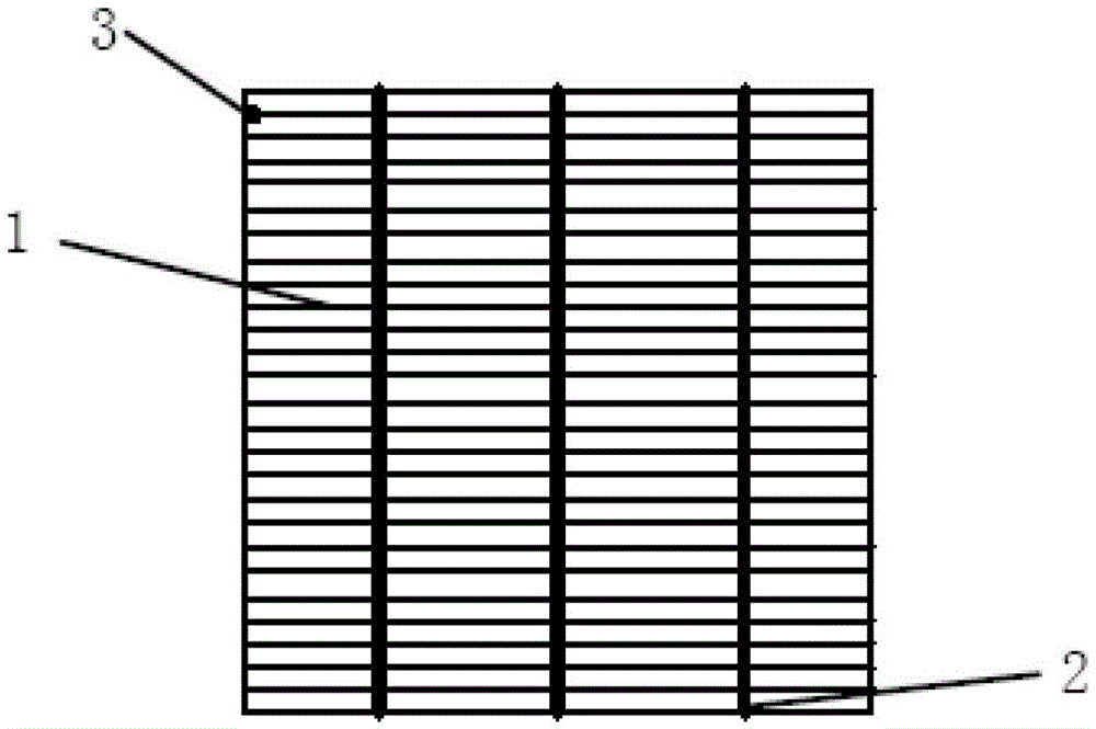
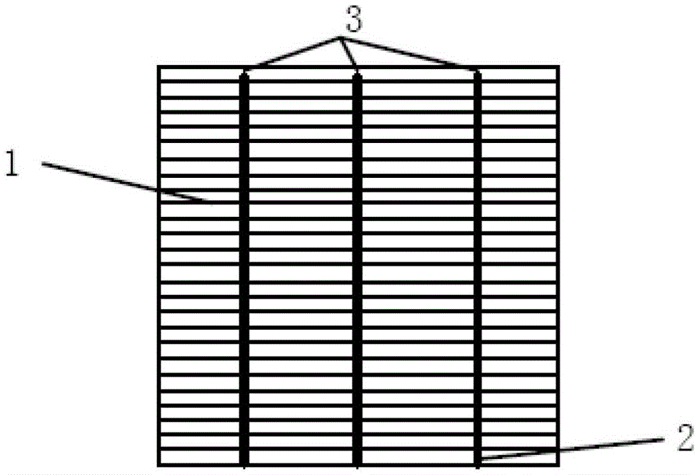
[0039] On the basis of Embodiment 1, a preferred embodiment of the present invention is: the first and second screens have directionality. Such as figure 1 and figure 2 As shown, the first and second screen plates can realize the directivity of the first and second screen plates by setting feature points at the ends of the fine grid and / or the main grid. Such as figure 1 As shown, the feature points can be the ends of the fine grid roughening. figure 2 In , the feature points are the ends of the main grid refinement.

Embodiment 3

[0041] On the basis of Embodiment 2, a preferred embodiment of the present invention is: the second optical imaging device is a three-dimensional imaging device capable of obtaining a three-dimensional image of the silicon wafer; the image analysis and recognition system is provided with a three-dimensional image analysis module, The three-dimensional image of the silicon chip transmitted from the three-dimensional camera device is identified and analyzed by the three-dimensional image analysis module, and the average depth of the groove on the silicon chip is calculated, and the average depth of the groove is calculated. transmitted to the controller of the grouting machine; the grouting machine is used to sizing the second screen, the controller is connected with the motion actuator for adjusting the sizing amount of the grouting machine, and according to the groove The average depth controls the motion of the motion actuator. The motion actuator here may be the piston actua...


PUM


Abstract

The invention relates to a method of manufacturing a precision-overprinted selective emitter cell. The method of the invention combines optical positioning and mechanical positioning, precision overprinting between corrosion agent printing and gate line printing is realized through optical positioning, and consistency of printing patterns between silicon wafers is ensured through mechanical position. In optical positioning, the overlapping precision of silicon wafers and a second screen printing plate is checked, and the precision of overprinting is ensured. The screen printing plate is designed into a directional screen printing plate, which enables printed silicon wafers to be directional, facilitates rapid positioning of silicon wafers on a second printing platform and improves the printing efficiency. A second optical camera is set into a three-dimensional camera device, and a three-dimensional image analysis module is arranged in an image analysis and identification system, the sizing amount can be adjusted according to the monitored depths of grooves on different silicon wafers, the precision of overprinting is further improved, and the photoelectric conversion efficiency of the cell is improved.

Description

technical field [0001] The invention relates to the field of solar cells, in particular to a method for manufacturing a selective emitter cell. Background technique [0002] In the current photovoltaic industry, the development of high-efficiency cell technology is the key to improving the efficiency of solar cells. One of the more mature high-efficiency battery technologies is the suspended emitter battery. Due to its structural advantages, selective emitter solar cells can simultaneously obtain high short-circuit current open-circuit voltage and fill factor, and thus have high conversion efficiency and become a research hotspot. Its structure has two main features: a heavily diffused region with a relatively high doping concentration and a deep junction is formed under and near the metal gate line; a light diffusion region with a relatively low doping concentration and a shallow junction is formed at other positions. On the one hand, this structure can reduce the contact...

Claims


Application Information

Patent Timeline
Patent Type & Authority Patents(China)
IPC IPC(8): H01L31/18
CPCB41F15/36B41F33/0036H01L31/022458H01L31/1804Y02E10/547Y02P70/50
Inventor 卢君马嫣明李向清
Owner JIANGSU AIDUO PV TECH
Why Eureka
Try Eureka