Silicon-based group III-V nanotubes and micro-tubes as well as preparation method thereof

A III-V and microtube technology, applied in the field of nanotube and microtube materials and their preparation, can solve the problems of tube structure defects, high control cost, uncontrollable and other problems, achieve controllable number of tube wall circles, and improve luminous quality , The effect of fast tube making speed

Active Publication Date: 2014-09-03
BEIJING UNIV OF POSTS & TELECOMM
View PDF4 Cites 12 Cited by
  • Summary
  • Abstract
  • Description
  • Claims
  • Application Information

AI Technical Summary

Problems solved by technology

[0015] The process of separating III-V nanotubes or microtubes from the host substrate using the above-mentioned transfer technology is relatively complicated, and it is easy to cause structural defects or mechanical deformation of the tubes
In particular, the ultrasonic process used in Solution casting can easily break or shatter the tube
In addition, the solution casting and SOS transfer processes are uncontrollable, and the positioning of nanotubes or microtubes on Si substrates cannot be realized
Although fiber optic tapered transfer can solve most of the problems of solution casting and SOS transfer, it can only transfer independent unsupported microtubes with a diameter of several microns, and the operation cost is high
[0016] In summary, the above methods for preparing nanotubes and microtubes on Si substrates are not ideal, especially the optical properties of the prepared Si-based nanotubes and microtubes are far from reaching the level of practical silicon-based photonic devices. basic requirements

Method used


Image

  • Silicon-based group III-V nanotubes and micro-tubes as well as preparation method thereof
  • Silicon-based group III-V nanotubes and micro-tubes as well as preparation method thereof
  • Silicon-based group III-V nanotubes and micro-tubes as well as preparation method thereof

Examples


Embodiment 1

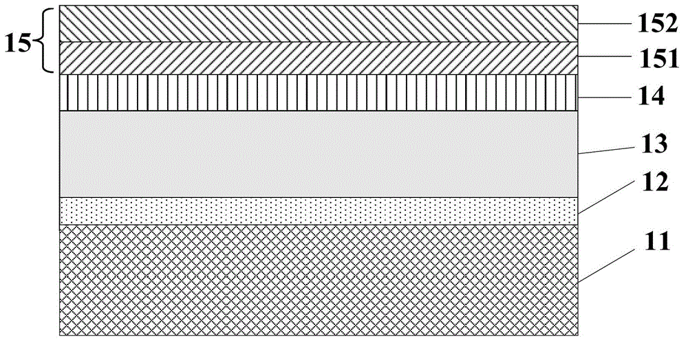
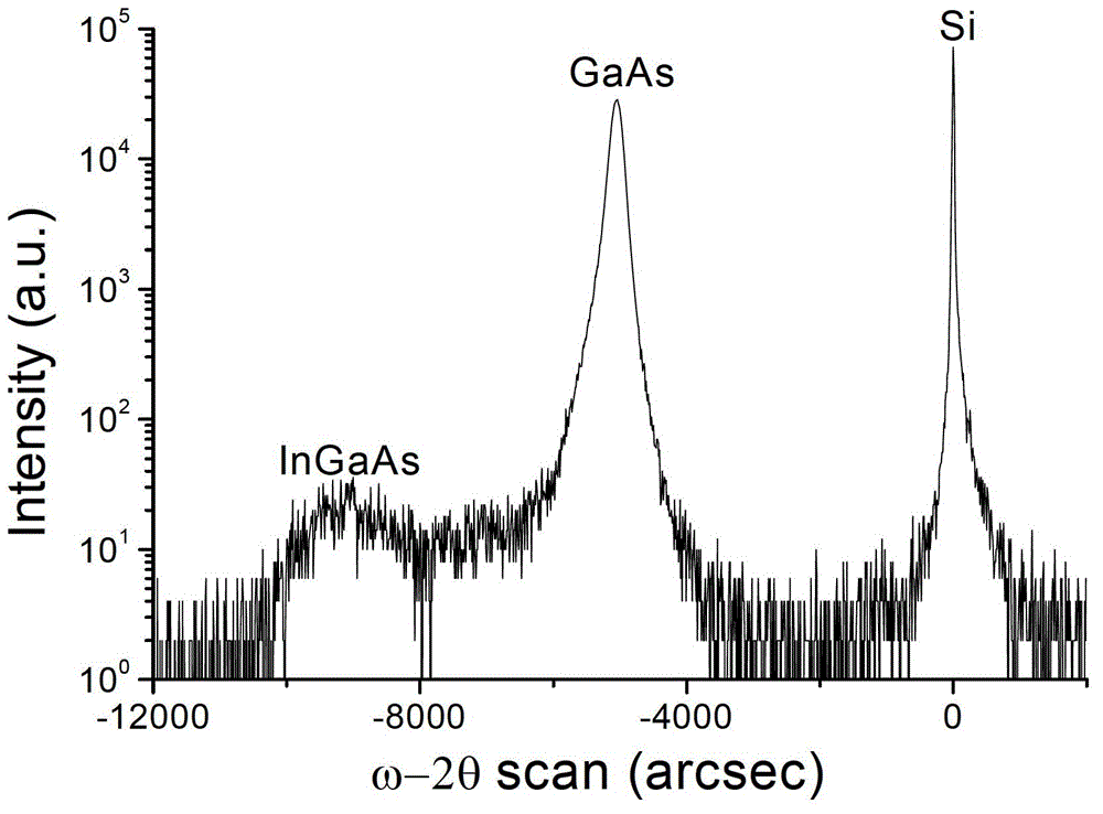
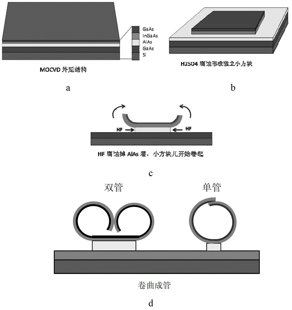
[0053]Embodiment 1: Preparation of III-V group InGaAs / GaAs microtubes on Si(100) substrate

[0054] S1: Clean the single crystal Si substrate and remove the oxide layer on the Si surface, and then epitaxially grow the abnormal buffer layer on the single crystal Si substrate;

[0055] RCA cleaning is performed on the Si sheet, and the oxide layer on the surface of the Si(100) substrate is removed by hydrofluoric acid (HF). Finally, the Si substrate is placed in the MOCVD reaction chamber after cleaning with deionized water and drying.

[0056] Warming up to 750°C, under H 2 Bake the Si sheet under the atmosphere for 30 minutes, and then pass the AsH at the same temperature 3 Passivate for 30 minutes.

[0057] Cool down to 420°C, using trimethyl (TMGa), arsine (AsH 3 ) to grow a low temperature GaAs nucleation layer (Low temperature GaAs nucleation layer), with a thickness of 70nm and a V / III ratio controlled at 250.

[0058] Heating up to 630°C, using TMGa, AsH 3 Grow an i...


PUM

PropertyMeasurementUnit
diameteraaaaaaaaaa
thicknessaaaaaaaaaa
thicknessaaaaaaaaaa

Abstract

The invention discloses silicon-based group III-V nanotubes and micro-tubes as well as a preparation method thereof. The nanotubes and the micro-tubes are of cylindrical hollow tubular structures with non-closed ends, which are formed by self-crimping of epitaxially grown group III-V strain semiconductor films on a single crystal Si substrate, the diameters of the nanotubes and the micro-tubes are 1 nm to 100 microns, and the lengths of the nanotubes and the micro-tubes are 1 micron to 1 mm. The tubular structures have great application value in the fields of silicon-based photonics, micro-machine systems and sensing. The invention integrates mutated epitaxial growth from bottom to top with a photoetching corrosion technology from top to bottom. Through lateral corrosion of group III-V sacrificial layers, the group III-V strain dual-layer films are released from Si and are crimped to tubes. The method is compatible with a process of group III-V photoelectron and micro-electronics devices and has the advantages of simple tube production process, good tube appearance, controllable tube size and the like, and furthermore, a large area of group III-V nanotube or micro-tube arrays with consistent rule are easily formed on the Si.

Description

technical field [0001] The invention relates to a nanotube and microtube material and a preparation method thereof, belonging to the field of semiconductor materials. Background technique [0002] In recent years, in the field of nanotechnology, especially in the field of nanomaterials, nanotubes and microtubes have attracted the attention of many researchers at home and abroad. The reason is that nanotubes and microtubes not only have excellent and unique structures, shapes, mechanical, mechanical, thermal, optical, and electrical properties, but also have many new physical laws and effects waiting to be discovered. Physical electronics, optics, biomedicine and other fields have shown very broad application prospects and important application value. Carbon nanotubes and microtubes are the earliest and most widely studied. Carbon nanotubes (Carbon nanotube, CNT) were first successfully prepared by Iijima et al. in 1991 [S.Iijima, Nature, 354(1991) 56]. Commonly used carbo...

Claims


Application Information

Patent Timeline
Patent Type & Authority Applications(China)
IPC IPC(8): B81B1/00B81C99/00
Inventor 王琦王二洋李伯昌任晓敏贾志刚闫映策蔡世伟黄永清
Owner BEIJING UNIV OF POSTS & TELECOMM
Why Eureka
Try Eureka