
Preparation method of RRAM (Resistive Random Access Memory)

A resistive memory and resistive switching technology, which is used in gaseous chemical plating, metal material coating process, electrical components, etc., can solve the problems that limit the wide application of ALD technology, the high resistance state resistance value changes in a large range, and the device resistance change is stable. It can improve the resistance switching characteristics, the erasing and writing voltage can be adjusted, and the high density can be achieved.

Inactive Publication Date: 2014-09-10
ZHEJIANG UNIV
View PDF5 Cites 4 Cited by
  • Summary
  • Abstract
  • Description
  • Claims
  • Application Information

AI Technical Summary

Problems solved by technology

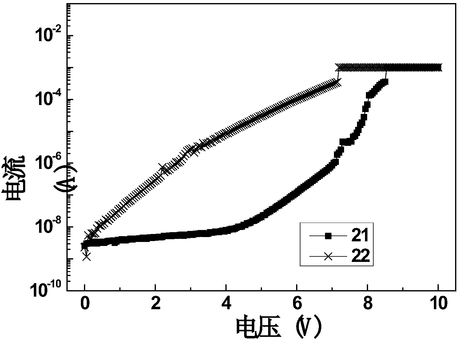
However, due to the high resistance of the AlN film, the device requires a very high activation voltage, resulting in poor resistance stability of the device, a large range of resistance in the high resistance state, and the device is easily broken down.
These all limit the wide application of ALD technology in the field of resistive memory

Method used


Image

  • Preparation method of RRAM (Resistive Random Access Memory)
  • Preparation method of RRAM (Resistive Random Access Memory)
  • Preparation method of RRAM (Resistive Random Access Memory)

Examples


Embodiment 1

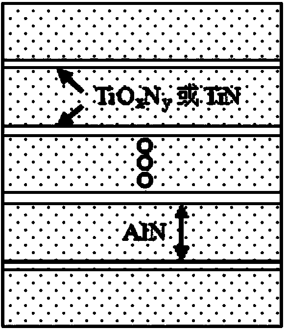
[0035] Aluminum nitride is used as the matrix of the resistive dielectric layer, and titanium oxynitride is used as the doped layer. Using titanium tetraisopropoxide as the second precursor, N 2 / H 2 (1:1) mixed gas plasma as a reactant, including the following steps:

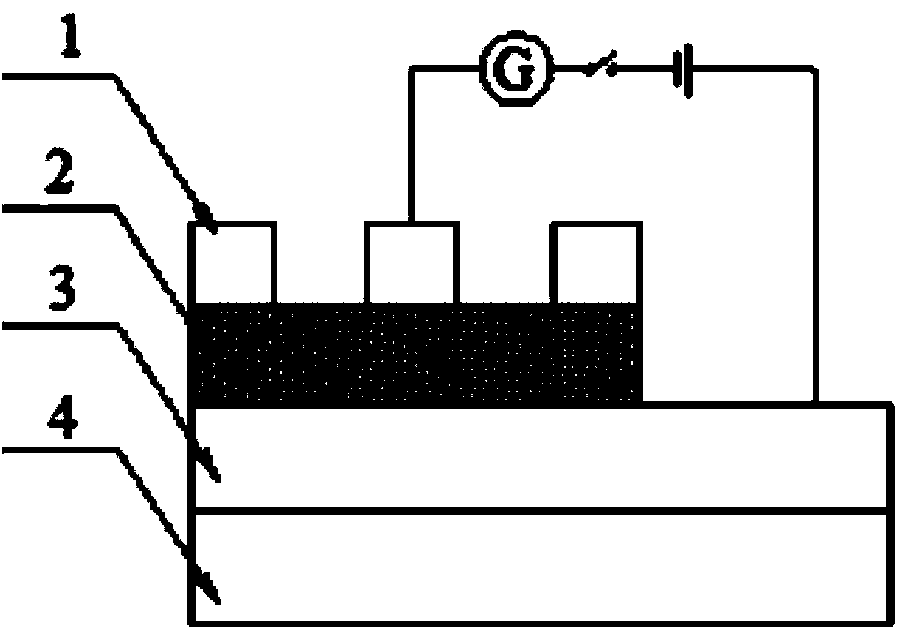
[0036] 1) Using magnetron sputtering method on SiO 2(300nm) / Si(100) substrate 4 surface preparation inert metal Pt bottom electrode 3, the bottom electrode 3 thickness of gained is 150nm, and the temperature of preparation is 150 ℃, and deposition main gas is argon gas, and pressure is 0.5Pa, and sputtering power It is 300W.

[0037] 2) Using plasma-enhanced atomic layer deposition, using trimethylaluminum as the first precursor and titanium tetraisopropoxide as the second precursor, N 2 / H 2 The plasma of (1:1) mixed gas is the first and the second reactant, and argon is used as the inert gas for cleaning, and the aluminum nitride layer matrix film of 2 cycles is deposited on the Pt bottom electrode 3 ear...

Embodiment 1-2

[0040] Other conditions are the same as embodiment 1-1, the first and second reactants are changed into N 2 / H 2 (5:1) mixed gas plasma, the number of cycles of the aluminum nitride layer matrix film is changed to 4, the thickness of the matrix layer is 0.32nm, and finally the single atomic layer titanium oxynitride doped aluminum nitride film (AlN :Ti=4:1).

Embodiment 2-1

[0050] Aluminum nitride is used as the substrate of the resistive dielectric layer, titanium nitride is used as the doped layer, tetrakis(dimethylamino)titanium is used as the second precursor, and N 2 / H 2 (1:5) mixed gas plasma as a reactant, including the following steps:

[0051] 1) The inert metal Au bottom electrode 3 was prepared on the surface of the quartz substrate 4 by magnetron sputtering. The obtained bottom electrode 3 had a thickness of 150 nm, the temperature of the preparation was 150° C., the main gas for deposition was argon, and the pressure was 0.5 Pa. The transmitting power is 300W.

[0052] 2) Using plasma-enhanced atomic layer deposition method, using trimethylaluminum as the first precursor and tetrakis(dimethylamino)titanium as the second precursor, N 2 / H 2 The plasma of (1:5) mixed gas is the first and the second reactant, and argon is used as the inert gas for cleaning, and the aluminum nitride layer matrix film of 9 cycles is deposited on the P...


PUM

PropertyMeasurementUnit
thicknessaaaaaaaaaa
thicknessaaaaaaaaaa
thicknessaaaaaaaaaa

Abstract

The invention relates to the field of semiconductors, and aims to provide a preparation method of a RRAM (Resistive Random Access Memory). The preparation method comprises the steps of assembling a bottom electrode, a resistance changeable medium layer and a top electrode on a substrate in sequence; the preparation of the material of the resistance changeable medium comprises the following steps of: carrying a first precursor, an inert gas, a first reactant and the inert gas into a reactor in sequence, and preparing multiple circulating film substrates by using a plasma enhanced atomic layer deposition technology; then carrying a second precursor, the inert gas, a second reactant and the inert gas into the reactor in sequence, and preparing a single circulating doping layer by using the plasma enhanced atomic layer deposition technology; carrying out the steps mentioned above circularly, alternately and sequentially to obtain the resistance-changeable medium layer. The preparation method of the RRAM can control the thickness of the film of the resistance-changeable medium layer precisely, the prepared film is high in conformality and density, and large-area uniformity can be realized.

Description

technical field [0001] The invention relates to the field of semiconductors, in particular to a preparation method of a resistive variable memory. Background technique [0002] With the development of the information industry, many new non-volatile storage devices have emerged, including ferroelectric memory, magnetic memory, phase change memory and resistive change memory (RRAM). Among these new memories, RRAM has broad application prospects due to its advantages of simple structure, low power consumption, fast read and write, and high-density storage. It is internationally recognized as a strong competitor for mainstream memory technologies below the 32nm node One of them is expected to become the next generation of "universal" non-volatile memory. [0003] RRAM utilizes the resistive switching characteristics of insulators or semiconductor materials to store information. The so-called resistive switch characteristic means that under the excitation of the pulse voltage, ...

Claims


Application Information

Patent Timeline
Patent Type & Authority Applications(China)
IPC IPC(8): H01L45/00C23C16/44
Inventor 张启龙张剑杨辉邬华宇
Owner ZHEJIANG UNIV
Learn More