Distributed local boron-doped double-face photoreceptive crystalline silicon solar cell and preparation method thereof
A solar cell, distributed technology, applied in photovoltaic power generation, circuits, electrical components, etc., can solve the problems of large overall doping area on the back side, reducing the area of passivation film, shallow doping depth, etc. The effect of improving the actual power generation performance and increasing the doping concentration
- Summary
- Abstract
- Description
- Claims
- Application Information
AI Technical Summary
Problems solved by technology
Method used
Image
Examples
Embodiment 1
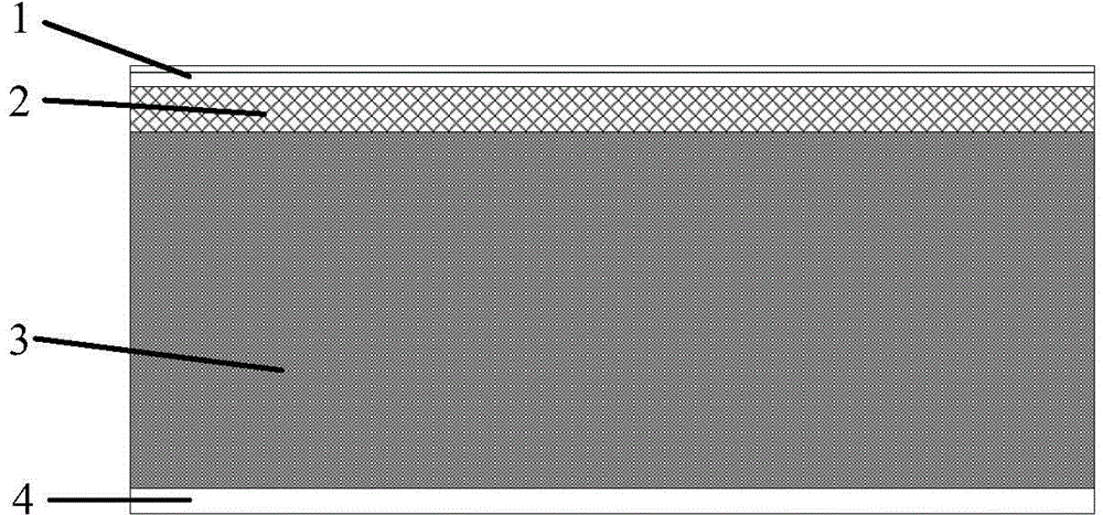
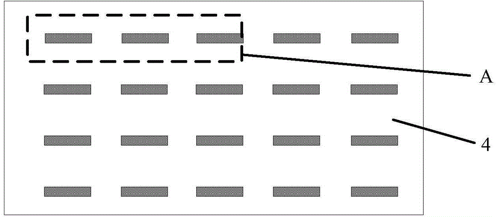
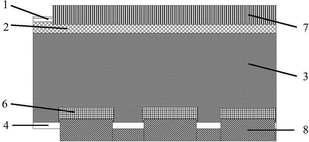
[0035] A method for preparing a distributed localized boron-doped double-sided photosensitive crystalline silicon solar cell provided in this embodiment, such as figure 1 As shown, on the P-type silicon substrate 3, after completing the preparation of the p-n junction N region, that is, the N-type doped region 2, the deposition of the front anti-reflection passivation film 1, and the deposition of the rear passivation film 4, The passivation film 4 on the back side is partially removed by laser, and the pattern is a distribution line pattern, such as figure 2 shown. The length of the short line is 2cm, the width is 60μm, the distance between the line and the center of the line along the direction of the short line is 2.2cm, and the distance between the line and the center of the line is 700μm in the direction perpendicular to the short line, and the silicon substrate is exposed after laser removal. , Print a layer of borosilicate paste with a thickness of 50 μm and a width o...
Embodiment 2
[0040] A method for preparing a distributed localized boron-doped double-sided photosensitive crystalline silicon solar cell provided in this embodiment, such as figure 1 As shown, on the p-type silicon substrate 3, the preparation of the p-n junction N region, that is, the N-type doped region 2, the deposition of the front anti-reflection passivation film 1, and the deposition of the rear passivation film 4 are completed. , use etching slurry to partially remove the passivation film 4 on the back surface, and the pattern is a distribution line pattern, such as figure 2 shown. The length of the short line is 0.5cm, the width is 55μm, the distance between the line and the center of the line along the direction of the short line is 1.2cm, and the distance between the line and the center of the line is 600μm in the direction perpendicular to the short line, and the silicon substrate is exposed after laser removal On 3, a layer of borosilicate paste with a thickness of 30 μm and...
PUM
| Property | Measurement | Unit |
|---|---|---|
| Doping concentration | aaaaa | aaaaa |
| Thickness | aaaaa | aaaaa |
| Width | aaaaa | aaaaa |
Abstract
Description
Claims
Application Information


