Light emitting diode epitaxial wafer and manufacture method thereof
A technology of light-emitting diodes and epitaxial wafers, applied in electrical components, circuits, semiconductor devices, etc., can solve the problems affecting the luminous efficiency of LEDs, lattice defects, etc., so as to improve the luminous efficiency of LEDs, reduce the density of line dislocations, and improve the growth quality. Effect
- Summary
- Abstract
- Description
- Claims
- Application Information
AI Technical Summary
Problems solved by technology
Method used
Image
Examples
Embodiment 1
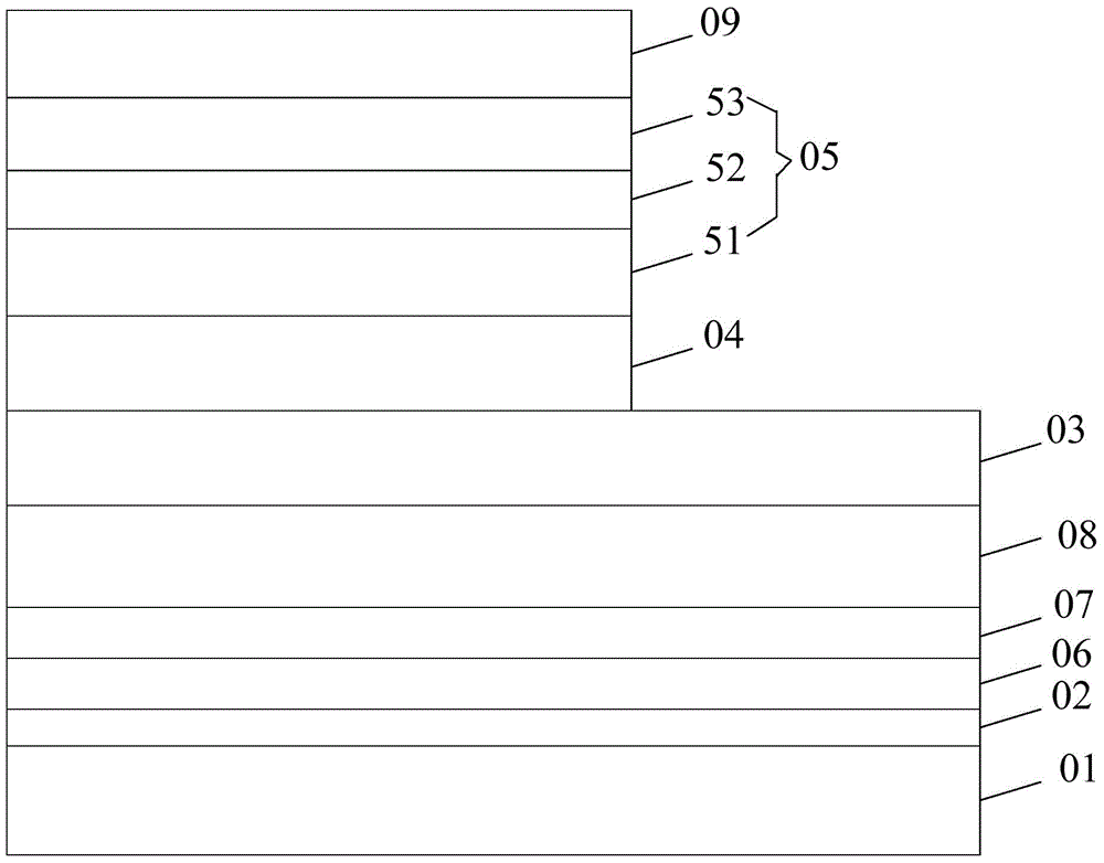
[0035] An embodiment of the present invention provides a light emitting diode epitaxial wafer, see figure 1 , the epitaxial wafer includes a substrate 01, a buffer layer 02, an N-type layer 03, a light-emitting layer 04, and a P-type layer 05 sequentially covering the substrate 01. The epitaxial wafer also includes a three-dimensional recrystallization layer 06, and a three-dimensional recrystallization layer 06 It grows between the buffer layer 02 and the N-type layer 03, and the three-dimensional recrystallization layer 06 is a GaN layer formed by segmented three-dimensional growth, and the growth pressure of each segment of the three-dimensional recrystallization layer is different.
[0036] Specifically, the substrate 01 can be Al with crystal orientation [0001] 2 o 3 Sapphire as the substrate.
[0037] Specifically, the buffer layer 02 is a GaN buffer layer with a thickness between 15 and 40 nm.
[0038] Specifically, the three-dimensional recrystallization layer 06 is...
Embodiment 2
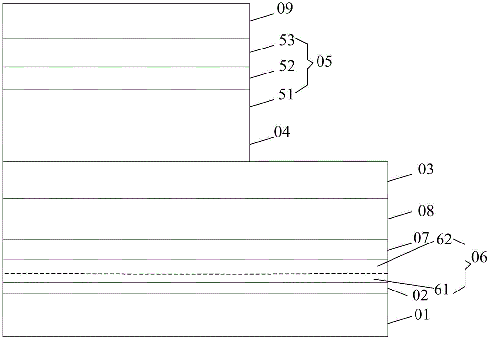
[0050] An embodiment of the present invention provides a light emitting diode epitaxial wafer, see figure 2 , the structure of the epitaxial wafer is similar to that of the embodiment, including a substrate 01, a buffer layer 02 covering the substrate 01, an N-type layer 03, a light-emitting layer 04, and a P-type layer 05, and the epitaxial wafer also includes a three-dimensional recrystallization layer 06 , the three-dimensional recrystallized layer 06 is grown between the buffer layer 02 and the N-type layer 03 .
[0051] The difference from the first embodiment is that the growth temperature of the three-dimensional recrystallized layer 06 is also limited in this embodiment. which is
[0052] In an implementation of the embodiment of the present invention, the three-dimensional recrystallization layer 06 includes: a first recrystallization sublayer 61 and a second recrystallization sublayer 62 grown at the same temperature but under different pressures, the first recryst...
Embodiment 3
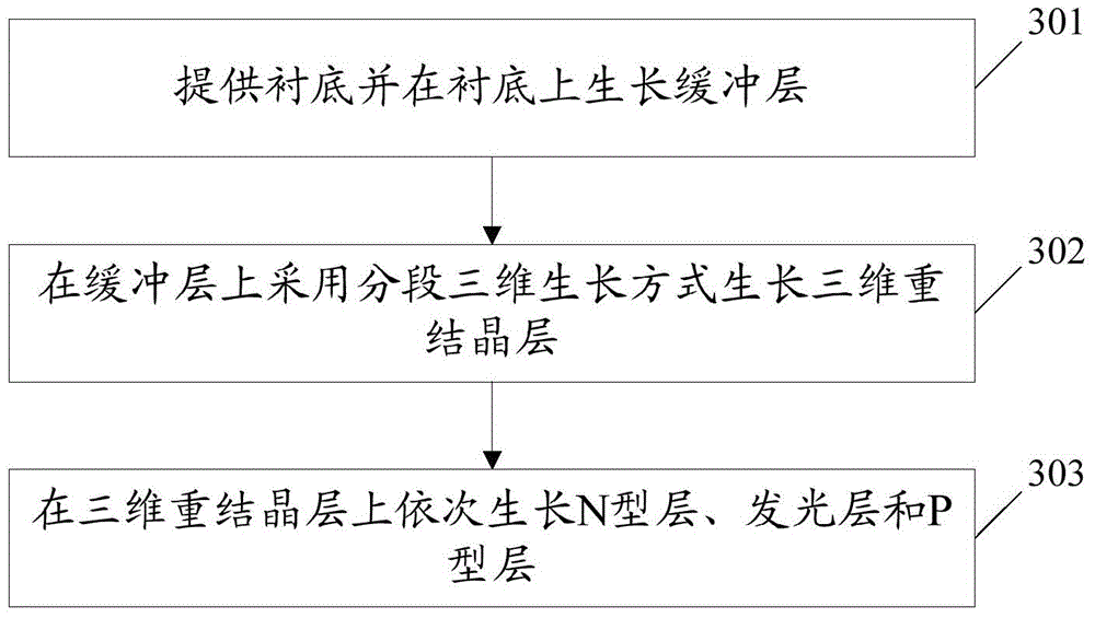
[0062] An embodiment of the present invention provides a method for manufacturing a light-emitting diode epitaxial wafer, which is applicable to the epitaxial wafer in Embodiment 1, see image 3 , the method includes:
[0063] Step 301: providing a substrate and growing a buffer layer on the substrate.
[0064] Specifically, the substrate is Al with a crystal orientation of [0001] 2 o 3 Sapphire is used as the substrate, and it is annealed in a hydrogen atmosphere for 1-10 minutes to clean the surface of the substrate, and then nitriding is performed at a temperature between 1000°C and 1200°C to form a thin layer of free state on the surface of the substrate Nitrogen is more favorable for buffer layer nucleation.
[0065] Specifically, the buffer layer is a GaN buffer layer with a thickness between 15 nm and 40 nm, a growth temperature between 400° C. and 600° C., and a growth pressure between 400 Torr and 600 Torr.
[0066] Step 302 : growing a three-dimensional recrystal...
PUM
 Abstract
Description
Claims
Application Information


