Organic semiconductor photoelectric device based on graphene electrode

A technology of organic semiconductors and graphene electrodes, which is applied in semiconductor devices, semiconductor/solid-state device manufacturing, electric solid-state devices, etc., and can solve problems such as large-area low-cost manufacturing, indium atomic diffusion, and incompatible production technologies.

Active Publication Date: 2014-10-08
CHONGQING INST OF GREEN & INTELLIGENT TECH CHINESE ACADEMY OF SCI
View PDF9 Cites 32 Cited by
  • Summary
  • Abstract
  • Description
  • Claims
  • Application Information

AI Technical Summary

Problems solved by technology

Traditional anodic indium tin oxide (ITO) has disadvantages such as shortage of indium resources, expensive indium resources, diffusion of indium atoms, and poor bending performance. , high preparation requirements and high production prices
The existing electrode preparation technology is not suitable for large-area and low-cost manufacturing due to problems such as material sources and preparation processes, especially incompatible with future efficient and cost-effective organic electronic device production technologies such as roll-to-roll

Method used


Image

  • Organic semiconductor photoelectric device based on graphene electrode
  • Organic semiconductor photoelectric device based on graphene electrode
  • Organic semiconductor photoelectric device based on graphene electrode

Examples


Embodiment 1

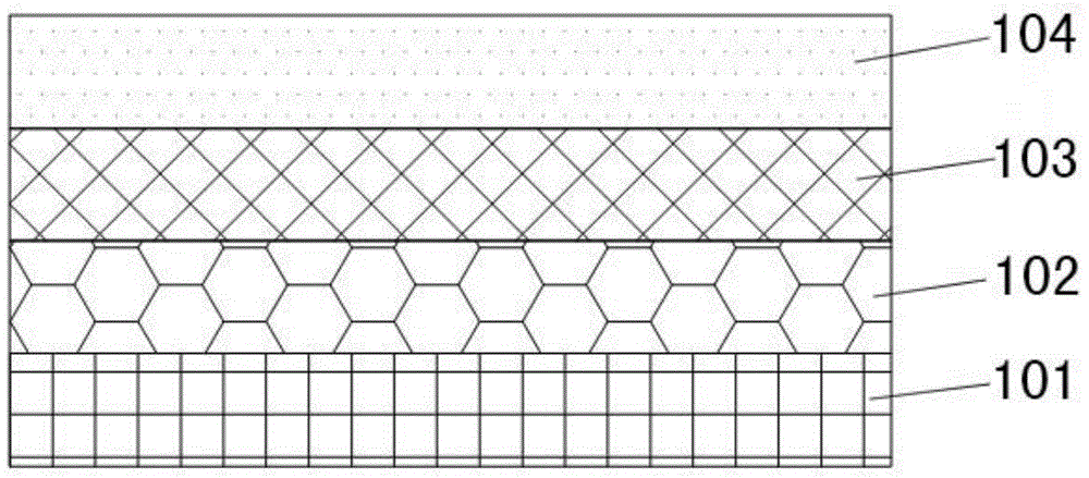
[0044] Embodiment 1: Preparation of graphene composite anode A

[0045] The float polished glass was cleaned with deionized water, acetone, and IPA for 20 minutes, and then dried with nitrogen gas as the substrate. Single-layer graphene was prepared by chemical vapor deposition, and a two-layer graphene film was obtained by multiple transfers. 3 Doped and transferred to a glass substrate. The silver grid was prepared by photolithography, the line spacing of the grid was set to 200 μm, and the line width was 5 μm, and then transferred to the graphene film. Then spin-coat a layer of PEDOT:PSS conductive polymer layer on the metal grid, heat treatment at 130°C for 10 minutes. The resulting graphene anode is as figure 1 As shown, the square resistance is 7Ω / □, the light transmittance is 86%, and the work function is 5.2eV.

Embodiment 2

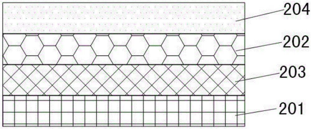
[0046] Embodiment 2: Preparation of graphene composite anode B

[0047] The PET was washed with deionized water, acetone, and IPA for 20 minutes, and then dried with nitrogen to serve as a substrate. A layer of silver film was sputtered on the PET, and the silver film on the PET was etched into a grid with a line spacing of 100 μm and a line width of 5 μm by photolithography. Single-layer graphene was prepared by chemical vapor deposition, and a three-layer graphene film was obtained by multiple transfers. 3 After doping, transfer to the metal grid. Then spin-coat a layer of PEDOT:PSS conductive polymer layer on the graphene film, heat treatment at 130°C for 10 minutes. The resulting graphene anode is as figure 2 As shown, the square resistance is 1.2Ω / □, the light transmittance is 80%, and the work function is 5.2eV.

[0048] Embodiment 3: preparation doping modified graphene cathode

[0049] The glass substrate was cleaned with ionized water, acetone, and IPA for 20 mi...

Embodiment 4

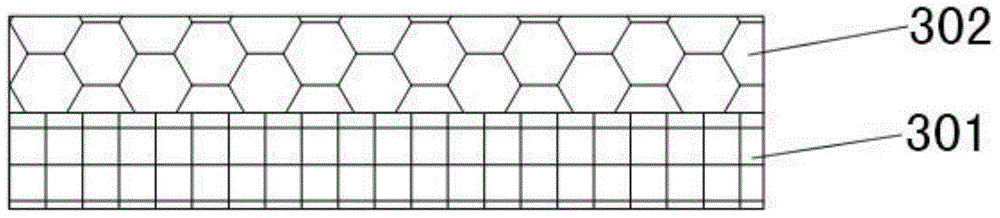
[0050] Embodiment 4: prepare the graphene negative electrode that is adsorbed with surface modification layer

[0051] The PET substrate was cleaned with ionized water, acetone, and IPA for 20 minutes, and then dried with nitrogen. Single-layer graphene was prepared by chemical vapor deposition, and two-layer graphene films were obtained by multiple transfers. Branched polyethyleneimine (PEI) was doped in ethylene glycol monomethyl ether solvent at a mass ratio of 0.4%. The prepared solution was spin-coated on the graphene film at a speed of 5000 rpm, and then heat-treated on a hot plate at 100° C. for 10 minutes to obtain a graphene cathode adsorbed with 10 nmPEI. The resulting graphene cathode is as Figure 4 As shown, its work function is 3.7eV.


PUM

PropertyMeasurementUnit
distanceaaaaaaaaaa
widthaaaaaaaaaa
thicknessaaaaaaaaaa

Abstract

The invention relates to an organic semiconductor photoelectric device based on a graphene electrode. The organic semiconductor photoelectric device comprises a graphene anode, a graphene cathode and an organic functional layer. The graphene anode is composed of a graphene film, a metal mesh and a conductive polymer layer. The graphene cathode is a graphene film on which a surface modification layer is absorbed. The organic semiconductor photoelectric device based on the graphene electrode has excellent performance on the aspects of sheet resistance, light transmittance and work functions, is suitable for large-scale low-cost manufacturing and compatible with a reel-to-reel technology and the like, and lays a foundation for large-scale low-cost flexible device production in the future.

Description

technical field [0001] The invention relates to an organic semiconductor photoelectric device based on a graphene electrode, belonging to the field of organic semiconductor photoelectric devices. Background technique [0002] Transparent electrodes are an important part of organic semiconductor optoelectronic devices, which include anode and cathode electrodes. Traditional anodic indium tin oxide (ITO) has disadvantages such as shortage of indium resources, expensive indium resources, diffusion of indium atoms, and poor bending performance. , high preparation requirements and high production prices. The existing electrode preparation technology is not suitable for large-area and low-cost manufacturing due to problems such as material sources and preparation processes, especially incompatible with future efficient and cost-effective organic electronic device production technologies such as roll-to-roll. [0003] Graphene is an advanced two-dimensional nanomaterial with exce...

Claims


Application Information

Patent Timeline
Patent Type & Authority Applications(China)
IPC IPC(8): H01L51/52H01L51/54H01L51/56H01L51/00
CPCH10K50/81
Inventor 史浩飞罗伟邵丽冷重钱杜春雷
Owner CHONGQING INST OF GREEN & INTELLIGENT TECH CHINESE ACADEMY OF SCI
Why Eureka
Try Eureka