
A kind of laser processing method of solder mask layer of circuit board

A laser processing method and circuit board technology, applied in printed circuit, metal processing, laser welding equipment, etc., can solve the problems of affecting the product yield, increasing the cost of the enterprise, and long product production cycle, so as to shorten the product production cycle, The effect of simplifying the production process and shortening the production cycle

Active Publication Date: 2016-06-15
ZHONGSHAN AISCENT TECH
View PDF6 Cites 0 Cited by
  • Summary
  • Abstract
  • Description
  • Claims
  • Application Information

AI Technical Summary

Problems solved by technology

[0011] (1) When exposing, it is necessary to cover the light-painted film on the circuit board layout to be exposed, and use UV light source for exposure. During the process, operations such as alignment and adjustment are required, and the productivity is low.
[0012] (2) During the exposure process, high-energy UV light sources cannot be used for exposure, and the exposure speed is slow
[0013] (3) The circuit board may be deformed during the preparation process, which will cause deviations between the alignment of the film graphics and the circuit board, and affect the yield of the product
[0014] (4) Developing operation is required, and waste water will be generated during the developing process, which is not environmentally friendly, and the post-treatment of waste water also increases the production cost of the enterprise
[0015] (5) Pre-baking and post-baking processes are required, the production cycle of the product is long, and the production process is cumbersome

Method used

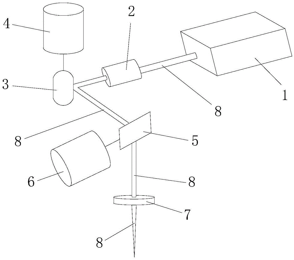
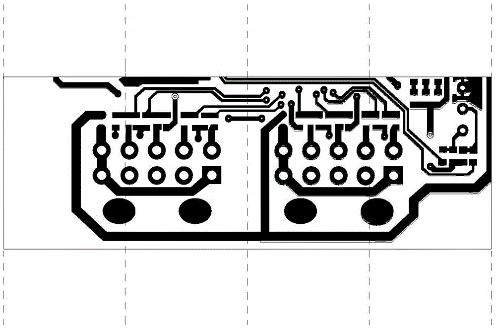

Image

  • A kind of laser processing method of solder mask layer of circuit board
  • A kind of laser processing method of solder mask layer of circuit board
  • A kind of laser processing method of solder mask layer of circuit board

Examples


Embodiment Construction

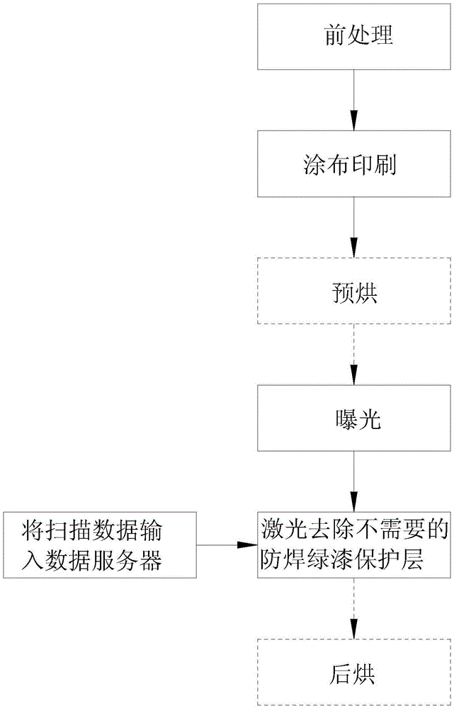
[0040] A kind of laser processing method of circuit board solder resist layer, with reference to figure 1 , the steps are as follows:

[0041] (1), pre-processing

[0042] Alcohol, ethyl acetate, acetone and other cleaning solutions are used to remove oxidation and oil stains on the surface of the circuit board. The pretreatment method of the present invention is the same as the pretreatment process and cleaning solvent used for the circuit board in the prior art.

[0043] (2), coating printing

[0044] Using electrostatic spraying or printing process, the solder resist green paint is coated and printed on the surface of the circuit board.

[0045] Solder resist green paint (liquid photo-induced solder resist, also known as green oil) is a protective layer that is coated on the circuit and substrate of the printed circuit board that do not need to be soldered. The purpose is to protect the formed circuit pattern for a long time. The main components include: epoxy and acryli...


PUM


Abstract

The invention discloses a method for machining a solder mask of a circuit board through a laser. The method comprises the step of performing preprocessing, coating printing and exposure and removing an unnecessary soldering preventing green paint protection layer through the laser. The development technology is replaced by the technology of removing the protection layer through the laser, waste water is not produced, environmental friendliness is achieved, energy is saved, and production cost of enterprises can be reduced. In the exposure step, the soldering preventing green paint protection layer can be directly exposed through a high-energy UV light source, the exposure speed is high, the whole face of the circuit board is directly irradiated in the exposure process, a light painting film shade does not need to be adopted, the pre-drying and post-drying steps can be omitted, the production technology is simplified, and the production cycle of products can be shortened. In the step of removing the unnecessary soldering preventing green paint protection layer through the laser, laser dynamic scanning is adopted, an image scanned by the laser can be dynamically adjusted according to deformation of the circuit board, and the quality of the products is improved.

Description

technical field [0001] The invention relates to a method for producing a circuit board, in particular to a method for processing a solder-proof protective layer of a circuit board. Background technique [0002] In the process of circuit board production, in order to protect the circuit on the circuit board, avoid short circuit phenomenon caused by scratches and achieve "solder proof" function, it is necessary to coat a protective film on the circuit board. The protective film in the prior art It is a protective layer of solder mask. [0003] The manufacturing process of the solder resist green paint protective layer in the prior art is as follows: [0004] (1) Pre-treatment to remove oxidation and oil to prevent pollution. [0005] (2) Coating and printing, using electrostatic spraying or printing process to coat and print the solder resist green paint on the surface of the circuit board. [0006] (3) Preliminary curing of the protective layer of the solder resist green p...

Claims


Application Information

Patent Timeline
Patent Type & Authority Patents(China)
IPC IPC(8): B23K26/70
CPCB23K26/0093B23K26/361B23K2101/42
Inventor 杜卫冲韩建崴
Owner ZHONGSHAN AISCENT TECH
Learn More